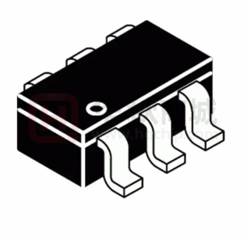
WD3136E
WD3136E
Http//: www.sh-willsemi.com
24V DC/DC Step-Up Regulator
Descriptions
The WD3136E is a high efficiency, high power, peak
current mode step-up converter integrated 32V power
MOSFET with 3A (Typ.) current limit. It could support
up to maximum 24V output.
The boost converter WD3136E runs in Pulse-Width
SOT-23-6L
Modulation (PWM) mode at 1MHz fixed switching
frequency to reduce output ripple and improve
external components. At light load, the converter enters
LX
1
GND
2
FB
3
WD3136E
conversion efficiency. It allows for the use of small
Skipping Mode to maintain a high efficiency over a wide
load current range. The build-in soft start circuitry
minimizes the inrush current at start-up.
The WD3136E is available in SOT-23-6L package.
6
NC
5
IN
4
EN
Standard product is Pb-free and Halogen-free.
Pin Configuration (Top View)
Features
Input Voltage Range
: 2.4V~20V
Reference Voltage
: 600mV
Switching Frequency
: 1MHz (Typ.)
Efficiency
: Up to 94%
Internal Compensation
Current Limit
: 3A (D=50%)
Low RDS(ON)
: 100mΩ
Automatic Pulse Skipping Modulation
Package
6
1
PDA, PMP, MP3
Digital Camera
2
3
3136 = Device code
DE= Special code
Applications
Cell Phone and Smart Phone
4
3136
DEYW
: SOT-23-6L
5
Y = Year code
W = Week code
Marking
Order Information
Will Semiconductor Ltd.
1
Device
Package
Shipping
WD3136E-6/TR
SOT-23-6L
3000/Reel & Tape
2020/06 - Rev. 1.0
�WD3136E
Typical Applications
L
D
VIN
VOUT=0.6*(1+R1/R2)
4.7μH~10μH
1
5
IN
R1
LX
WD3136E FB
CIN
10μF
4
ON
OFF
EN
GND
3
COUT
10μF
R2
1kΩ~10kΩ
2
Pin Descriptions
Symbol
Pin No.
Descriptions
LX
1
Switch Node
GND
2
Ground
FB
3
Feedback
EN
4
Enable
IN
5
Power Supply
NC
6
No Connection
Block Diagram
OVP
VIN
UVLO
Thermal
Shutdown
Current
Sense
PWM
COMP
Regulator
ISENSE
NC
Reference
&
Bias
Enable
Control
Will Semiconductor Ltd.
PWM
Logic
Driver
OSC
1MHz
FB
Low-Pass
Filter
VREF
EN
Limiting
LX
gm
Error
Amplifier
VREF
Soft
Start
GND
2
2020/06 - Rev. 1.0
�WD3136E
Absolute Maximum Ratings
Parameter
Symbol
Value
Unit
VIN Pin Voltage Range
VIN
-0.3~28
V
EN Pin Voltage Range
VEN
-0.3~28
V
LX Pin Voltage Range (DC)
VLX
-0.3~32
V
FB Pin Voltage Range
VFB
-0.3~6
Junction To Ambient Thermal Resistance – SOT-23-6L (Note 1)
Operating Junction Temperature
Lead Temperature(Soldering, 10s)
RθJA
90
TJ
-40~150
o
260
o
-55~150
o
TL
Storage Temperature
V
o
Tstg
C/W
C
C
C
These are stress ratings only. Stresses exceeding the range specified under “Absolute Maximum Ratings” may
cause substantial damage to the device. Functional operation of this device at other conditions beyond those
listed in the specification is not implied and prolonged exposure to extreme conditions may affect device
reliability.
Note 1: Thermal Resistance (θJA) is measured with the component mounted on 1.5inch x 1.5inch, 2layers,
FR4 test board with 1.0inch x 1.0inch copper area of 2oz in top layer, and in still air condition.
ESD Ratings
Parameter
Symbol
Value
Unit
HBM
4000
V
CDM
2000
V
Symbol
Value
Unit
VIN
2.4~20
V
VOUT
VIN~24
V
L
4.7~10
μH
CIN
10 (Typ.)
μF
COUT
10 (Typ.)
μF
Resistance Between FB Pin And GND
R2
1~10
kΩ
Operating Ambient Temperature
TA
-40~85
o
Operating Junction Temperature
TJ
-40~125
o
Electrostatic Discharge
Recommended Operating Conditions
Parameter
Input Voltage Range
Output Voltage Range
Inductor
Input Capacitor
Output Capacitor
C
C
These values are recommended values that have been successfully tested in several applications. Other
values may be acceptable in other applications but should be fully tested by the user.
Will Semiconductor Ltd.
3
2020/06 - Rev. 1.0
�WD3136E
Electronics Characteristics
(Ta=25 oC, VIN=3V, L=4.7μH, CIN=COUT=10μF, unless otherwise noted)
Parameter
Symbol
Test Condition
Min
Typ
Max
Units
20
V
2.39
V
Basic Operation
Operation Voltage Range
VIN
Under Voltage Lockout
VUVLO
UVLO Hysteresis
VHYS
Quiescent Current
IQ
2.4
VIN Rising
2.2
No Switching
VFB=0.7V
0.1
V
0.25
mA
mA
Supply Current
IS
Switching at no load
0.5
Shutdown Current
ISD
VEN
很抱歉,暂时无法提供与“WD3136E-6/TR”相匹配的价格&库存,您可以联系我们找货
免费人工找货- 国内价格
- 5+1.31112
- 50+1.01726
- 150+0.89144
- 500+0.73430
- 国内价格
- 1+0.89870
- 200+0.69080
- 1500+0.60170
- 3000+0.55990
