AGM312M2
● General Description
The AGM312M2 combines advanced trench
MOSFET technology with a low resistance package
to provide extremely low RDS(ON) .
This device is ideal for load switch and battery
protection applications.
● Features
Product Summary
BVDSS
RDSON
ID
30V
18mΩ
9A
-30V
40mΩ
-6.8A
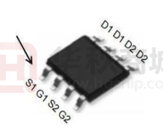
SOP-8 Pin Configuration
■ Advance high cell density Trench technology
■ Low RDS(ON) to minimize conductive loss
■ Low Gate Charge for fast switching
■ Low Thermal resistance
D1
G1
● Application
D2
G2
■ MB/VGA Vcore
■ SMPS 2nd Synchronous Rectifier
■ POL application
■ BLDC Motor driver
S1
S2
Package Marking and Ordering Information
Device Marking
Device
Device Package
Reel Size
Tape width
Quantity
AGM312M2
AGM312M2
SOP8
--mm
--mm
3000
Table 1. Absolute Maximum Ratings (TA=25℃)
Rating
Symbol
Parameter
N-Ch
P-Ch
Units
VDS
Drain-Source Voltage (VGS=0V)
30
-30
V
VGS
Gate-Source Voltage (VDS=0V)
±20
±20
V
9
-6.8
A
7.65
-5.78
A
Drain Current-Continuous@ Current-Pulsed (Note 2)
40
-40
A
Total Power Dissipation(Tc=25℃)
3.1
3.2
W
Total Power Dissipation(Tc=70℃)
0.7
0.7
W
1.28
1.28
mJ
Drain Current-Continuous(Tc=25℃) (Note 1)
ID
IDM (pluse)
PD
EAS
TJ,TSTG
Drain Current-Continuous(Tc=70℃)
Avalanche energy (Note 3)
Operating Junction and Storage Temperature Range
-55 To 150
-55 To 150
Typ
Max
Unit
℃
Table 2. Thermal Characteristic
Symbol
Parameter
RθJA
Thermal Resistance Junction-ambient (Steady State)1
---
62.5
℃/W
RθJC
Thermal Resistance Junction-Case1
---
--
℃/W
www.agm-mos.com
1
VER2.5
�AGM312M2
Table 3. N- Channel Electrical Characteristics (TA=25℃unless otherwise noted)
Symbol
Parameter
Conditions
Min
Typ
Max
Unit
On/Off States
BVDSS
Drain-Source Breakdown Voltage
VGS=0V ID=250μA
30
--
--
V
IDSS
Zero Gate Voltage Drain Current
VDS=30V,VGS=0V
--
--
1
μA
IGSS
Gate-Body Leakage Current
VGS=±12V,VDS=0V
--
--
±100
nA
VGS(th)
Gate Threshold Voltage
VDS=VGS,ID=250μA
1.0
--
2.0
V
gFS
Forward Transconductance
VDS=15V,ID=6.8A
--
27
--
S
RDS(on)
Drain-Source On-State Resistance
VGS=10V, ID=6.8A
--
18
--
mΩ
VGS=4.5V, ID=6.6A
--
24
21
mΩ
--
510
--
pF
--
95
--
pF
--
33
--
pF
0.3
1.1
2.3
Ω
--
4
8
nS
--
10
17
nS
--
16
22
nS
Dynamic Characteristics
Ciss
Input Capacitance
Coss
Output Capacitance
Crss
Reverse Transfer Capacitance
Rg
Gate resistance
VDS=20V,VGS=0V,
F=1MHZ
VGS=0V,
VDS=0V,f=1.0MHz
Switching Times
td(on)
Turn-on Delay Time
tr
Turn-on Rise Time
td(off)
Turn-Off Delay Time
tf
Turn-Off Fall Time
--
5
9
nS
Qg
Total Gate Charge
--
5.8
7
nC
Qgs
Gate-Source Charge
--
1.6
--
nC
Qgd
Gate-Drain Charge
--
1.4
--
nC
--
--
2.6
A
VGS=10V,VDS=20V,
ID=5.4A,RGEN=1Ω,
RL=3.7Ω
VGS=4.5V,
VDS=20V, ID=10A
Source-Drain Diode Characteristics
ISD
Source-Drain Current(Body Diode)
VSD
Forward on Voltage
VGS=0V,IS=5.4A
--
0.81
1.2
V
trr
Reverse Recovery Time
IF=5A , dI/dt=100A/µs ,
--
12
25
ns
Qrr
Reverse Recovery Charge
TJ=25℃
--
10
17
nc
Notes 1.The maximum current rating is package limited.
Notes 2.Repetitive Rating: Pulse width limited by maximum junction temperature
Notes 3.EAS condition: TJ=25℃
www.agm-mos.com
2
VER2.5
�AGM312M2
Table 3. P-Channel Electrical Characteristics (TA=25℃unless otherwise noted)
Symbol
Parameter
Conditions
Min
Typ
Max
Unit
On/Off States
BVDSS
Drain-Source Breakdown Voltage
VGS=0V ID=-250μA
-30
--
--
V
IDSS
Zero Gate Voltage Drain Current
VDS=-30V,VGS=0V
--
--
-1
μA
IGSS
Gate-Body Leakage Current
VGS=±12V,VDS=0V
--
--
±100
nA
VGS(th)
Gate Threshold Voltage
VDS=VGS,ID=-250μA
-1.0
--
-2.0
V
gFS
Forward Transconductance
VDS=-15V,ID=-6.7A
--
-25
--
S
RDS(on)
Drain-Source On-State Resistance
VGS=-10V, ID=-8A
--
40
--
mΩ
VGS=-4.5V, ID=-5A
--
50
--
mΩ
--
620
--
pF
--
115
--
pF
--
57
--
pF
1.2
5.7
9.6
Ω
--
10
--
nS
--
9
--
nS
--
23
--
nS
Dynamic Characteristics
Ciss
Input Capacitance
Coss
Output Capacitance
Crss
Reverse Transfer Capacitance
Rg
Gate resistance
VDS=-20V,VGS=0V,
F=1MHZ
VGS=0V,
VDS=0V,f=1.0MHz
Switching Times
td(on)
Turn-on Delay Time
tr
Turn-on Rise Time
td(off)
Turn-Off Delay Time
tf
Turn-Off Fall Time
--
10
--
nS
Qg
Total Gate Charge
--
16
22
nC
Qgs
Gate-Source Charge
--
4.3
--
nC
Qgd
Gate-Drain Charge
--
7
--
nC
--
--
-2.6
A
-0.77
-1.2
V
VGS=-10V,VDS=-20V,
ID=-10A,RGEN=1Ω
RL=2Ω
VGS=-4.5V,
VDS=-20V, ID=-10A
Source-Drain Diode Characteristics
ISD
Source-Drain Current(Body Diode)
VSD
Forward on Voltage
VGS=0V,IS=-2A
--
trr
Reverse Recovery Time
IF=-5A , dI/dt=100A/µs ,
--
31
57
ns
Qrr
Reverse Recovery Charge
TJ=25℃
--
29
47
nc
Notes 1.The maximum current rating is package limited.
Notes 2.Repetitive Rating: Pulse width limited by maximum junction temperature
Notes 3.EAS condition: TJ=25℃
www.agm-mos.com
3
VER2.5
�AGM312M2
N-CHANNEL TYPICAL CHARACTERISTICS (25 °C, unless otherwise noted)
40
10
VGS = 10 V thru 4 V
8
ID - Drain Current (A)
ID - Drain Current (A)
30
VGS = 3 V
20
6
TC = 25 °C
4
10
2
TC = 125 °C
0
TC = - 55 °C
0
0
0.5
1
1.5
VDS - Drain-to-Source Voltage (V)
2
0.6
1.8
2.4
1.2
VGS - Gate-to-Source Voltage (V)
0
3
Transfer Characteristics
Output Characteristics
1000
0.030
C - Capacitance (pF)
RDS(on) - On-Resistance (Ω)
800
0.025
VGS = 4.5 V
0.020
VGS = 8 V
600
Ciss
400
VGS = 10 V
0.015
200
Crss
Coss
0
0.010
0
10
20
30
0
40
10
20
30
VDS - Drain-to-Source Voltage (V)
ID - Drain Current (A)
Capacitance
On-Resistance vs. Drain Current and Gate Voltage
10
1.8
ID = 6.8 A
8
RDS(on) - On-Resistance (Normalized)
ID = 6.8 A
VGS - Gate-to-Source Voltage (V)
40
VDS = 32 V
6
VDS = 20 V
VDS = 10 V
4
2
3
6
9
12
VGS = 10 V; 4.5 V
1.4
1.2
1.0
0.8
0.6
- 50
0
0
1.6
15
- 25
0
25
50
75
100
125
Qg - Total Gate Charge (nC)
TJ - Junction Temperature (°C)
Gate Charge
On-Resistance vs. Junction Temperature
www.agm-mos.com
4
150
VER2.5
�AGM312M2
N-CHANNEL TYPICAL CHARACTERISTICS (25 °C, unless otherwise noted)
100
0.05
RDS(on) - On-Resistance (Ω)
IS - Source Current (A)
ID = 6.8 A
TJ = 150 °C
10
TJ = 25 °C
1
0.1
0.04
TJ = 125 °C
0.03
TJ = 25 °C
0.02
0.01
0.0
0.3
0.6
0.9
1.2
VSD - Source-to-Drain Voltage (V)
0
2
4
6
8
VGS - Gate-to-Source Voltage (V)
Source-Drain Diode Forward Voltage
On-Resistance vs. Gate-to-Source Voltage
10
60
1.9
48
Power (W)
VGS(th) (V)
1.6
ID = 250 μA
1.3
36
24
1
12
0.7
- 50
- 25
0
25
50
75
100
125
0
0.001
150
0.01
TJ - Temperature (°C)
Threshold Voltage
0.1
Time (s)
1
10
Single Pulse Power, Junction-to-Ambient
100
Limited by RDS(on)*
ID - Drain Current (A)
10
100 μs
1 ms
1
10 ms
100 ms
0.1
TA = 25 °C
Single Pulse
BVDSS Limited
1s
10 s
DC
0.01
0.1
1
10
100
VDS - Drain-to-Source Voltage (V)
* VGS > minimum VGS at which RDS(on) is specified
Safe Operating Area, Junction-to-Ambient
www.agm-mos.com
5
VER2.5
�AGM312M2
N-CHANNEL TYPICAL CHARACTERISTICS (25 °C, unless otherwise noted)
10
ID - Drain Current (A)
8
6
4
2
0
0
25
50
75
100
125
150
TC - Case Temperature (°C)
Current Derating*
4
1.25
1.0
Power (W)
Power (W)
3
2
0.75
0.50
1
0.25
0
0.0
0
25
50
75
100
125
150
0
TC - Case Temperature (°C)
50
75
100
125
150
TA - Ambient Temperature (°C)
Power Derating, Junction-to-Foot
www.agm-mos.com
25
Power Derating, Junction-to-Ambient
6
VER2.5
�AGM312M2
N-CHANNEL TYPICAL CHARACTERISTICS (25 °C, unless otherwise noted)
1
Normalized Effective Transient
Thermal Impedance
Duty Cycle = 0.5
0.2
Notes:
0.1
0.1
PDM
0.05
t1
t2
1. Duty Cycle, D =
t1
t2
2. Per Unit Base = R thJA = 120 °C/W
0.02
3. T JM - T A = PDMZthJA(t)
Single Pulse
0.01
10 -4
10 -3
4. Surface Mounted
10 -2
10 -1
1
100
10
1000
Square Wave Pulse Duration (s)
Normalized Thermal Transient Impedance, Junction-to-Ambient
1
Normalized Effective Transient
Thermal Impedance
Duty Cycle = 0.5
0.2
0.1
0.1
0.05
0.02
0.01
10 -4
Single Pulse
10 -3
10 -2
10 -1
Square Wave Pulse Duration (s)
1
10
Normalized Thermal Transient Impedance, Junction-to-Foot
www.agm-mos.com
7
VER2.5
�AGM312M2
P-CHANNEL TYPICAL CHARACTERISTICS (25 °C, unless otherwise noted)
40
10
V GS = 10 V thru 4 V
8
ID - Drain Current (A)
ID - Drain Current (A)
32
24
16
V GS = 3 V
6
4
T C = 25 °C
8
2
T C = 125 °C
0
0.0
T C = - 55 °C
V GS = 2 V
0.5
1.0
1.5
2.0
VDS - Drain-to-Source Voltage (V)
0
0
2.5
1
2
3
4
VGS - Gate-to-Source Voltage (V)
Output Characteristics
5
Transfer Characteristics
1000
0.090
C - Capacitance (pF)
RDS(on) - On-Resistance (Ω)
800
0.070
VGS = 4.5 V
0.050
VGS = 8 V
VGS = 10 V
0.030
600
Ciss
400
200
Coss
Crss
0
0.010
0
10
20
ID - Drain Current (A)
30
40
24
32
8
16
VDS - Drain-to-Source Voltage (V)
0
On-Resistance vs. Drain Current and Gate Voltage
Capacitance
1.8
10
ID = 8 A
RDS(on) - On-Resistance (Normalized)
ID = 10 A
VGS - Gate-to-Source Voltage (V)
40
8
V DS = 20 V
6
V DS = 10 V
V DS = 30 V
4
2
9
18
27
36
45
Qg - Total Gate Charge (nC)
Gate Charge
www.agm-mos.com
V GS = 10 V
1.4
V GS = 4.5 V
1.2
1.0
0.8
0.6
- 50
0
0
1.6
- 25
0
25
50
75
100
TJ - Junction Temperature (°C)
125
150
On-Resistance vs. Junction Temperature
8
VER2.5
�AGM312M2
P-CHANNEL TYPICAL CHARACTERISTICS (25 °C, unless otherwise noted)
0.15
100
ID = 8 A
0.12
RDS(on) - On-Resistance (Ω)
IS - Source Current (A)
10
T J = 150 °C
1
0.1
T J = 25 °C
0.09
0.06
T J = 125 °C
0.03
0.01
T J = 25 °C
0.001
0.0
0.00
0.2
0.4
0.6
0.8
1.0
VSD - Source-to-Drain Voltage (V)
0
1.2
1
3
2
4
5
6
7
8
10
9
VGS - Gate-to-Source Voltage (V)
Source-Drain Diode Forward Voltage
On-Resistance vs. Gate-to-Source Voltage
0.8
50
40
ID = 250 μA
Power (W)
VGS(th) Variance (V)
0.5
ID = 5 mA
0.2
30
20
- 0.1
10
- 0.4
- 50
- 25
0
25
50
75
100
125
0
0.001
150
TJ - Temperature (°C)
0.1
Time (s)
Threshold Voltage
Single Pulse Power, Junction-to-Ambient
0.01
1
10
100
Limited by RDS(on) *
ID - Drain Current (A)
10
1 ms
1
10 ms
100 ms
0.1
TA = 25 °C
Single Pulse
BVDSS Limited
1s
10 s
DC
0.01
0.01
0.1
1
10
VDS - Drain-to-Source Voltage (V)
* VGS > minimum VGS at which RDS(on) is specified
100
Safe Operating Area, Junction-to-Ambient
www.agm-mos.com
9
VER2.5
�AGM312M2
P-CHANNEL TYPICAL CHARACTERISTICS (25 °C, unless otherwise noted)
10
ID - Drain Current (A)
8
6
4
2
0
0
25
100
50
75
TC - Case Temperature (°C)
125
150
4.0
1.5
3.2
1.2
2.4
0.9
Power (W)
Power (W)
Current Derating*
1.6
0.8
0.6
0.3
0.0
0.0
0
25
75
100
50
TC - Case Temperature (°C)
125
150
0
Power Derating, Junction-to-Foot
25
75
100
125
50
TA - Ambient Temperature (°C)
150
Power Derating, Junction-to-Ambient
* The power dissipation PD is based on TJ(max) = 150 °C, using junction-to-case thermal resistance, and is more useful in settling the upper
dissipation limit for cases where additional heatsinking is used. It is used to determine the current rating, when this rating falls below the package
limit.
www.agm-mos.com
10
VER2.5
�AGM312M2
P-CHANNEL TYPICAL CHARACTERISTICS (25 °C, unless otherwise noted)
1
Normalized Effective Transient
Thermal Impedance
Duty Cycle = 0.5
0.2
0.1
Notes:
0.1
PDM
0.05
t1
t2
1. Duty Cycle, D =
0.02
t1
t2
2. Per Unit Base = R thJA = 110 °C/W
3. T JM - TA = PDMZthJA(t)
Single Pulse
0.01
10 -4
10 -3
10 -2
4. Surface Mounted
10 -1
1
Square Wave Pulse Duration (s)
100
10
1000
Normalized Thermal Transient Impedance, Junction-to-Ambient
1
Normalized Effective Transient
Thermal Impedance
Duty Cycle = 0.5
0.2
0.1
0.1
0.05
0.02
Single Pulse
0.01
10 -4
10 -3
10 -2
10 -1
Square Wave Pulse Duration (s)
1
10
Normalized Thermal Transient Impedance, Junction-to-Foot
www.agm-mos.com
11
VER2.5
�AGM312M2
●Dimensions(SOP8)
SYMBOL
min
TYP
max
SYMBOL
min
max
A
4.80
5.00
C
1.30
1.50
A1
0.37
0.47
C1
0.55
0.75
A2
1.27
C2
0.55
0.65
A3
0.41
C3
0.05
0.20
0.19
B
5.80
6.20
C4
B1
3.80
4.00
D
B2
www.agm-mos.com
5.00
D1
12
0.20
0.23
1.05
0.40
0.62
VER2.5
�AGM312M2
Disclaimer:
The information provided in this document is believed to be accurate and reliable.
however,Shenzhen Core Control Electronics Technology Co., Ltd. does not assume
any responsibility for the following consequencesDo not consider the use of such
information or use beyond its scope.
The information mentioned in this document may be changed at any time without
notice.
The products and information provided in this document do not infringe patents.
Shenzhen Core Control Electronics Technology Co., Ltd. assumes no responsibility
for any infringement of any other rights of third parties.The result of using such
products and information.
This document is the second version issued on May 10, 2022. This document
replaces andReplace all previously provided information.
It is a registered trademark of Shenzhen Core Control Electronics
Technology Co., Ltd.
Copyright © 2017 Shenzhen Core Control Electronics Technology Co., Ltd. all rights
reserved.
www.agm-mos.com
13
VER2.5
�