AGM6035A
● General Description
Product Summary
The AGM6035A combines advanced trench MOSFET
technology with a low resistance package to provide
extremely low RDS(ON) .
This device is ideal for load switch and battery
protection applications.
● Features
■ Advance
■ Low
RDS(ON) to minimize conductive loss
Gate Charge for fast switching
■ Low
Thermal resistance
RDSON
ID
60V
2.4mΩ
100A
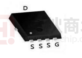
PDFN5*6 Pin Configuration
high cell density Trench technology
■ Low
BVDSS
● Application
■ MB/VGA Vcore
■ SMPS
■ POL
2nd Synchronous Rectifier
application
■ BLDC
Motor driver
Package Marking and Ordering Information
Device Marking
Device
Device Package
AGM6035A
AGM6035A
PDFN5*6
Table 1.
Reel Size
Tape width
Quantity
----
3000
----
Absolute Maximum Ratings (TA=25℃)
Parameter
Symbol
Value
Unit
VDS
Drain-Source Voltage (VGS=0V)
60
V
VGS
Gate-Source Voltage (VDS=0V)
±20
V
Drain Current-Continuous(Tc=25℃) (Note 1)
100
A
Drain Current-Continuous(Tc=100℃)
86
A
Drain Current-Continuous@ Current-Pulsed (Note 2)
270
A
Maximum Power Dissipation(Tc=25℃)
83
w
Maximum Power Dissipation(Tc=100℃)
33
w
Avalanche energy (Note 3)
200
mJ
-55 To 150
℃
Max
Unit
ID
IDM (pluse)
PD
EAS
TJ,TSTG
Table 2.
Operating Junction and Storage Temperature Range
Thermal Characteristic
Symbol
Typ
Parameter
RθJA
Thermal Resistance Junction-ambient (Steady State)1
---
55
℃/W
RθJC
Thermal Resistance Junction-Case1
---
1.5
℃/W
www.agm-mos.com
1
VER2.5
�AGM6035A
Table 3.
Electrical Characteristics (TA=25℃unless otherwise noted)
Symbol
Parameter
Conditions
Min
Typ
Max
Unit
On/Off States
BVDSS
Drain-Source Breakdown Voltage
VGS=0V ID=250μA
60
--
--
V
IDSS
Zero Gate Voltage Drain Current
VDS=48V,VGS=0V
--
--
1
μA
IGSS
Gate-Body Leakage Current
VGS=±20V,VDS=0V
--
--
±100
nA
VGS(th)
Gate Threshold Voltage
VDS=VGS,ID=250μA
1.0
1.6
2.5
V
gFS
Forward Transconductance
VDS=5V,ID=12A
--
65
--
S
RDS(on)
Drain-Source On-State Resistance
VGS=10V, ID=20A
--
2.4
3.0
mΩ
VGS=4.5V, ID=7A
--
3.3
4.2
mΩ
--
2800
--
pF
--
1170
--
pF
--
68
--
pF
--
1.1
--
Ω
--
20
--
nS
--
9.0
--
nS
--
60
--
nS
Dynamic Characteristics
Ciss
Input Capacitance
Coss
Output Capacitance
Crss
Reverse Transfer Capacitance
Rg
Gate resistance
VDS=30V,VGS=0V,
F=100MHZ
VGS=0V,
VDS=0V,f=1.0MHz
Switching Times
td(on)
Turn-on Delay Time
tr
Turn-on Rise Time
td(off)
Turn-Off Delay Time
tf
Turn-Off Fall Time
--
15
--
nS
Qg
Total Gate Charge
--
59
--
nC
Qgs
Gate-Source Charge
--
15
--
nC
Qgd
Gate-Drain Charge
--
10
--
nC
--
--
100
A
VGS=10V,VDS=30V,
ID=20A,RGEN=3.3Ω
VGS=10V, VDS=30V,
ID=20A
Source-Drain Diode Characteristics
ISD
Source-Drain Current(Body Diode)
VSD
Forward on Voltage
VGS=0V,IS=20A
--
--
1.0
V
trr
Reverse Recovery Time
IS=20A , dI/dt=100A/µs ,
--
24
--
ns
Qrr
Reverse Recovery Charge
TJ=25℃
--
84
--
nc
Notes 1.The maximum current rating is package limited.
Notes 2.Repetitive Rating: Pulse width limited by maximum junction temperature
Notes 3.EAS condition: TJ=25℃
www.agm-mos.com
2
VER2.5
�AGM6035A
Typical Characteristics
Fig.1 Typical Output Characteristics
Fig.2 On-Resistance vs G-S Voltage
Fig.3 Diode Forward Voltage vs. Current
Fig.4 Gate-Charge Characteristics
Fig.5 Normalized VGS(th) vs TJ
Fig.6 Normalized RDSON vs TJ
www.agm-mos.com
3
VER2.5
�AGM6035A
Fig.8 Safe Operating Area
Fig.7 Capacitance
Normalized Thermal Response (RθJC)
1
DUTY=0.5
0.2
0.1
0.1
0.05
0.02
0.01
0.01
P DM
SINGLE
T ON
T
D = TON/T
TJpeak = TC+P DMXRθJC
0.001
0.00001
0.0001
0.001
0.01
0.1
1
10
t , Pulse Width (s)
Fig.9 Normalized Maximum Transient Thermal Impedance
EAS=
VDS
90%
BVDSS
1
L x IAS2 x
2
BVDSS
BVDSS-VDD
VDD
IAS
10%
VGS
Td(on)
Tr
Ton
Td(off)
Tf
Toff
VGS
Fig.10 Switching Time Waveform
www.agm-mos.com
Fig.11 Unclamped Inductive Switching Waveform
4
VER2.5
�AGM6035A
H
D2
D
L1
Dimensions:PDFN5*6
SYMBOL
A
MILLIMETER
MIN
Typ.
MAX
0.900
1.000
1.100
A1
A2
k
L
E2
E
E1
L2
D1
e
b
0~0.05
D
4.824
4.900
4.976
D1
3.910
4.010
4.110
D2
4.924
5.000
5.076
E
5.924
6.000
6.076
E1
3.375
3.475
3.575
E2
5.674
5.750
5.826
b
0.350
0.400
0.450
e
1.270 TYP.
L
0.534
L1
0.424
d
L2
0.686
0.500
0.576
k
1.190
1.290
1.390
H
0.549
0.625
0.701
1.200
1.300
d
5
0.610
1.800 REF.
1.100
A
A1
A2
www.agm-mos.com
0.254 REF.
0.100
VER2.5
�AGM6035A
Disclaimer:
The information provided in this document is believed to be accurate and reliable.
however,Shenzhen Core Control Electronics Technology Co., Ltd. does not assume
any responsibility for the following consequencesDo not consider the use of such
information or use beyond its scope.
The information mentioned in this document may be changed at any time without
notice.
The products and information provided in this document do not infringe patents.
Shenzhen Core Control Electronics Technology Co., Ltd. assumes no responsibility
for any infringement of any other rights of third parties.The result of using such
products and information.
This document is the second version issued on September 10, 2022. This
document replaces andReplace all previously provided information.
It is a registered trademark of Shenzhen Core Control Electronics
Technology Co., Ltd.
Copyright © 2017 Shenzhen Core Control Electronics Technology Co., Ltd. all rights
reserved.
www.agm-mos.com
6
VER2.5
�
很抱歉,暂时无法提供与“AGM6035A”相匹配的价格&库存,您可以联系我们找货
免费人工找货- 国内价格
- 1+2.02500
- 10+1.95000
- 100+1.77000
- 500+1.68000