CT3400M
N-CHANNEL ENHANCEMENT
MODE POWER MOSFET
»Features
■
■
■
■
Fast Switching Characteristic
Low Gate Charger
Small Footprint & Low Peofile Package
RoHS Compliant & Halogen-Free
BVDSS
RDS(ON)typ
30V
22mΩ
5.8A
ID
»Description
CT3400M is from Coretong innovated design and silicon process technology to
achieve the lowest possible on- resistance and fast switching performance. It
provides the designer with an extreme efficient device for use in a wide range of
The SOT-23 package is widely preferred for commercial-industrial surface mount
applications and suited for low voltage applications such as DC/DC converters.
»Schematic & PIN Configuration
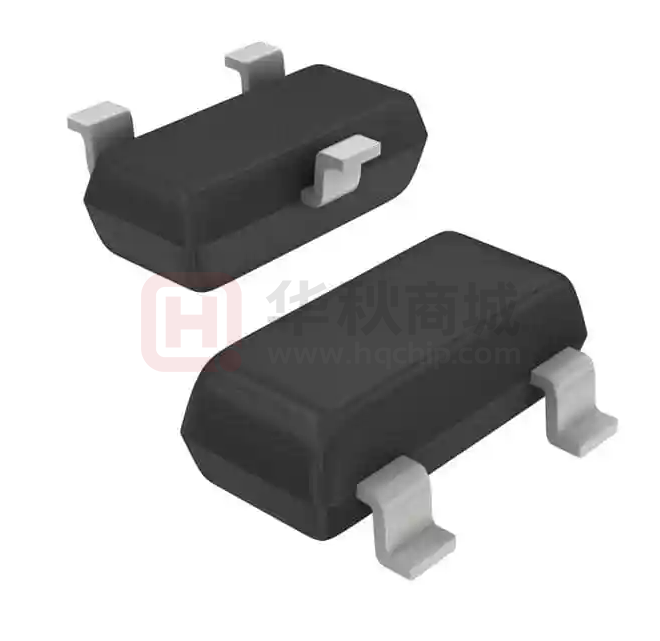
SOT-23
»Absolute Maximum Ratings@Tj=25oC(unless otherwise specified)
Symbol
VDS
VGS
ID@TA=25℃
ID@TA=70℃
IDM
Parameter
Drain-Source Voltage
Gate-Source Voltage
Drain Current, VGS @ 10V3
Drain Current, VGS @ 10V3
Pulsed Drain Current1
PD@TA=25℃ Total Power Dissipation3
TSTG
Storage Temperature Range
Operating Junction Temperature Range
TJ
»Thermal Data
Symbol
Rthj-a
Parameter
Maximum Thermal Resistance, Junction-ambient3
www.coretong.com
Rating
30
±12
5.8
4.8
20
0.4
-55 to 150
150
Units
V
V
A
A
A
W
Value
62.5
Unit
℃/W
℃
℃
1/4
�CT3400M
N-CHANNEL ENHANCEMENT
MODE POWER MOSFET
»Electrical Characteristics@Tj=25 oC(unless otherwise specified)
Symbol
BVDSS
RDS(ON)
Parameter
Test Conditions
Drain-Source Breakdown Voltage
Static Drain-Source On-Resistance2
Min.
Typ.
Max.
Units
VGS=0V, ID=250uA
30
-
-
V
VGS=10V, ID=5.8A
-
22
35
mΩ
VGS=4.5V, ID=5A
-
25
40
mΩ
VGS=2.5V, ID=4A
-
37
52
mΩ
0.7
0.95
1.2
V
VGS(th)
Gate Threshold Voltage
VDS=VGS, ID=250uA
gfs
Forward Transconductance
VDS=5V, ID=5A
8
-
-
S
IDSS
Drain-Source Leakage Current
VDS=30V, VGS=0V
-
-
1
uA
IGSS
Gate-Source Leakage
VGS=±12V, VDS=0V
-
-
±100
nA
Qg
Qgs
Total Gate Charge2
-
17.25
-
nC
-
2.1
-
nC
Qgd
Gate-Drain ("Miller") Charge
ID=5A
VDS=10V
VGS=6V
-
2
-
nC
td(on)
Turn-on Delay Time
-
4.4
-
ns
tr
td(off)
Rise Time
-
28.2
-
ns
-
16.2
-
ns
tf
Ciss
Fall Time
-
26
-
ns
-
630
-
pF
Coss
Output Capacitance
-
55
-
pF
Crss
Reverse Transfer Capacitance
VGS=0V
VDS=25V
f=1.0MHz
-
71
-
pF
Rg
Gate Resistance
f=1.0MHz
-
1.9
-
Ω
Min.
Typ.
Max.
Units
-
-
1.2
V
Gate-Source Charge
VDS=15V
ID=5A
RG=3Ω
VGS=10V
Turn-off Delay Time
Input Capacitance
»Source-Drain Diode
Symbol Parameter
VSD
Forward On Voltage²
Test Conditions
IS=1A, VGS=0V
Notes:
1.Pulse width limited by Max. junction temperature.
2.Pulse test
3.Surface mounted on 1 in2 2oz copper pad of FR4 board, t
很抱歉,暂时无法提供与“CT3400M”相匹配的价格&库存,您可以联系我们找货
免费人工找货- 国内价格
- 5+0.16675
- 20+0.15140
- 100+0.13606
- 500+0.12071
- 1000+0.11355
- 2000+0.10844