v
RTL8811CU-CG
Single-Chip IEEE 802.11a/b/g/n/ac 1T1R
WLAN with USB 2.0 Interface
DATASHEET
(CONFIDENTIAL: Development Partners Only)
Rev. 0.1r05 , July, 2016
Track ID:
Realtek Semiconductor Corp.
No. 2, Innovation Road II, Hsinchu Science Park, Hsinchu 300, Taiwan
Tel.: +886-3-578-0211. Fax: +886-3-577-6047
www.realtek.com
�RTL8811CU
Datasheet
COPYRIGHT
© 2016 Realtek Semiconductor Corp. All rights reserved. No part of this document may be reproduced,
transmitted, transcribed, stored in a retrieval system, or translated into any language in any form or by any
means without the written permission of Realtek Semiconductor Corp.
DISCLAIMER
Realtek provides this document “as is”, without warranty of any kind. Realtek may make improvements
and/or changes in this document or in the product described in this document at any time. This document
could include technical inaccuracies or typographical errors.
TRADEMARKS
Realtek is a trademark of Realtek Semiconductor Corporation. Other names mentioned in this document are
trademarks/registered trademarks of their respective owners.
USING THIS DOCUMENT
This document is intended for the software engineer’s reference and provides detailed programming
information.
Though every effort has been made to ensure that this document is current and accurate, more information
may have become available subsequent to the production of this guide.
REVISION HISTORY
Revision
0.1
0.1r05
Release Date
2016/07/27
2016/9/06
Summary
Preliminary release.
Modify general description and features
Single-Chip 802.11 a/b/g/n/ac 1T1R WLAN Controller
with USB 2.0 Interface
ii
Track ID:
Rev. 0.1r05
�RTL8811CU
Datasheet
Table of Contents
1.
GENERAL DESCRIPTION .............................................................................................................................................. 1
2.
FEATURES ......................................................................................................................................................................... 3
3.
APPLICATION DIAGRAMS ........................................................................................................................................... 5
3.1.
4.
PIN ASSIGNMENTS ......................................................................................................................................................... 6
4.1.
5.
PACKAGE IDENTIFICATION ........................................................................................................................................... 6
PIN DESCRIPTIONS ........................................................................................................................................................ 7
5.1.
5.2.
5.3.
5.4.
5.5.
5.6.
5.7.
5.8.
6.
11AC DUAL-BAND 1X1 RF APPLICATION .................................................................................................................... 5
POWER ON TRAP PIN .................................................................................................................................................... 7
USB TRANSCEIVER INTERFACE ................................................................................................................................... 7
EEPROM INTERFACE .................................................................................................................................................. 7
RF INTERFACE ............................................................................................................................................................. 8
LED INTERFACE .......................................................................................................................................................... 8
POWER MANAGEMENT HANDSHAKE INTERFACE ......................................................................................................... 9
CLOCK AND OTHER PINS.............................................................................................................................................. 9
POWER PINS ................................................................................................................................................................. 9
ELECTRICAL AND THERMAL CHARACTERISTICS ........................................................................................... 11
6.1.
TEMPERATURE LIMIT RATINGS .................................................................................................................................. 11
6.2.
DC CHARACTERISTICS ............................................................................................................................................... 11
6.2.1. Power Supply Characteristics ............................................................................................................................. 11
6.2.2. Digital IO Pin DC Characteristics ....................................................................................................................... 11
7.
INTERFACE TIMING SPECIFICATION .................................................................................................................... 12
7.1.
8.
MECHANICAL DIMENSIONS...................................................................................................................................... 13
8.1.
9.
USB BUS TIMING DURING POWER ON SEQUENCE ..................................................................................................... 12
MECHANICAL DIMENSIONS NOTES ............................................................................................................................ 14
ORDERING INFORMATION ........................................................................................................................................ 15
Single-Chip 802.11 a/b/g/n/ac 1T1R WLAN Controller
with USB 2.0 Interface
iii
Track ID:
Rev. 0.1r05
�RTL8811CU
Datasheet
List of Tables
TABLE 1.
TABLE 2.
TABLE 3.
TABLE 4.
TABLE 5.
TABLE 6.
TABLE 7.
TABLE 8.
TABLE 9.
TABLE 10.
TABLE 11.
TABLE 12.
TABLE 13.
TABLE 14.
POWER-ON TRAP PINS ............................................................................................................................................ 7
USB TRANSCEIVER INTERFACE .............................................................................................................................. 7
EEPROM INTERFACE .............................................................................................................................................. 7
RF INTERFACE ......................................................................................................................................................... 8
LED INTERFACE...................................................................................................................................................... 8
POWER MANAGEMENT HANDSHAKE INTERFACE ..................................................................................................... 9
CLOCK AND OTHER PINS ......................................................................................................................................... 9
POWER PINS .......................................................................................................................................................... 10
TEMPERATURE LIMIT RATINGS ............................................................................................................................. 11
DC CHARACTERISTICS .......................................................................................................................................... 11
3.3V GPIO DC CHARACTERISTICS ....................................................................................................................... 11
THE TYPICAL TIMING RANGE ................................................................................................................................. 12
PACKAGE DIMENSIONS NOTES .............................................................................................................................. 14
ORDERING INFORMATION...................................................................................................................................... 15
List of Figures
FIGURE 1.
FIGURE 2.
FIGURE 3.
FIGURE 4.
DUAL-BAND MIMO 1X1 SOLUTION(11AC 1X1 MAC/BB/RF + PA) SOLUTION --- RTL8811CU-CG .................... 5
PIN ASSIGNMENTS ................................................................................................................................................... 6
RTL8811CU-CG USB BUS POWER ON SEQUENCE .............................................................................................. 12
PACKAGE DIMENSION ........................................................................................................................................... 13
Single-Chip 802.11 a/b/g/n/ac 1T1R WLAN Controller
with USB 2.0 Interface
iv
Track ID:
Rev. 0.1r05
�RTL8811CU
Datasheet
1.
General Description
The Realtek RTL8811CU-CG is a highly-integrated IEEE 802.11 a/b/g/n/ac MAC/Baseband/RF WLAN
single chip. For Wireless LAN (WLAN) operation, it supports 1-stream 802.11ac solution with Multi-user
MIMO (Multiple-Input, Multiple-Output) STA mode with USB2.0 network interface controller.
The RTL8811CU-CG baseband implements multiuser Multiple-Input Multiple-Output (MIMO)
Orthogonal Frequency Division Multiplexing (OFDM) STA mode with one transmit and one receive path
(1T1R). Features include one spatial stream transmission, short Guard Interval (GI) of 400ns, spatial
spreading, and support for variant channel bandwidths. Moreover, RTL8811CU-CG provides one spatial
stream Space-Time Block Code (STBC) and Low Density Parity Check (LDPC) to extend the range of
transmission. As the recipient, the RTL8811CU-CG also supports explicit sounding packet feedback that
helps senders with beamforming capability.
For legacy compatibility, Direct Sequence Spread Spectrum (DSSS), Complementary Code Keying (CCK)
and OFDM baseband processing are included to support all IEEE 802.11a, 802.11b and 802.11g data rates.
Differential phase shift keying modulation schemes, DBPSK and DQPSK with data scrambling capability,
are available. CCK provides support for legacy data rates, with long or short preamble. The high speed
FFT/IFFT paths are combined with BPSK, QPSK, 16QAM, 64QAM and 256QAM modulation of the
individual subcarriers. The compatible coding rate of 1/2, 2/3, 3/4, and 5/6 provides up to 433.3Mbps for
IEEE 802.11ac with MIMO-OFDM.
The RTL8811CU-CG builds in an enhanced signal detector, an adaptive frequency domain equalizer, and a
soft-decision Viterbi decoder to alleviate severe multi-path effects and mutual interference in the reception
of multiple streams.
Receive vector diversity for multi-stream application is implemented for efficient utilization of the MIMO
channel. Efficient IQ-imbalance, DC offset, phase noise, frequency offset, and timing offset compensations
are provided for the radio frequency front-end.
The RTL8811CU-CG supports fast receiver Automatic Gain Control (AGC) with synchronous and
asynchronous control loops among antennas, antenna diversity functions, and adaptive transmit power
control functions to obtain better performance in the analog portions of the transceiver.
The RTL8811CU-CG MAC supports 802.11e for multimedia applications, 802.11i and WAPI (Wireless
Authentication Privacy Infrastructure) for security, and 802.11n/ac for enhanced MAC protocol efficiency.
Protocol efficiency is significantly improved by using packet aggregation techniques, such as A-MPDU
with BA and A-MSDU. Power saving mechanisms, such as Legacy Power Save, U-APSD, and MIMO, can
reduce the power wasted during idle time. They can also compensate for the extra power required to
Single-Chip 802.11 a/b/g/n/ac 1T1R WLAN Controller
with USB 2.0 Interface
1
Track ID:
Rev. 0.1r05
�RTL8811CU
Datasheet
transmit MIMO-OFDM. The RTL8811CU-CG provides simple legacy and 20MHz/40MHz/80MHz
co-existence mechanism to ensure backward and network compatibility.
Single-Chip 802.11 a/b/g/n/ac 1T1R WLAN Controller
with USB 2.0 Interface
2
Track ID:
Rev. 0.1r05
�RTL8811CU
Datasheet
2.
Features
General Information
56pins QFN
CMOS MAC, Baseband PHY and RF in a
single chip for IEEE 802.11a/b/g/n/ac
compatible WLAN
Support 802.11ac 1x1,Wave-2 compliant
with MU-MIMO STA mode
Complete 802.11n MIMO solution for
2.4GHz and 5Ghz band
Maximum PHY data rate up to 86.7Mbps
using 20MHz bandwidth, 200Mbps using
40MHz bandwidth, and 433.3Mbps using
80MHz bandwidth.
Backward compatible with 802.11a/b/g
devices while operating at 802.11n data rates
Backward compatible with 802.11a/n
devices while operating at 802.11ac data
rates.
Host Interface
Complies with
controller
USB LPM/Selective Suspend supported
USB
2.0 for
WLAN
Standards Supported
IEEE 802.11a/b/g/n/ac compatible WLAN
IEEE 802.11k Radio Resource Measurement
IEEE 802.11e QoS Enhancement (WMM)
WAPI (Wireless Authentication Privacy
Infrastructure) certified.
IEEE 802.11i (WPA, WPA2). Open, shared
key, and pair-wise key authentication
services
Cisco Compatible Extensions (CCX) for
WLAN devices
IEEE 802.11h DFS, TPC, Spectrum
Measurement
MAC Features
Frame aggregation for increased MAC
efficiency (A-MSDU, A-MPDU)
PHY-level spoofing to enhance legacy
compatibility
Low
latency
immediate
Acknowledgement (BA)
Channel management and co-existence
Long NAV for media reservation with
CF-End for NAV release
Multiple BSSID feature allows the
RTL8811CU-CG to assume multiple MAC
identities when used as a wireless bridge
Block
Single-Chip 802.11 a/b/g/n/ac 1T1R WLAN Controller
with USB 2.0 Interface
3
Track ID:
Rev. 0.1r05
�RTL8811CU
Datasheet
Transmit Opportunity (TXOP) Short
Inter-Frame Space (SIFS) bursting for higher
multimedia bandwidth
WiFi Direct supports wireless peer to peer
applications.
WiFi NAN (Neighborhood Area Network)
support
WiFi FTM (Fine Time Measurement)
supported
WiFi TDLS (Tunneled Direct Link Setup)
Supported
Support Network List Offload
CCA on secondary through RTS/CTS
handshake.
Support TCP/UDP/IP checksum offload
Other Features
Supports Wake-On-WLAN
Packet and Wake-up frame
via
Magic
Transmit Beamforming
Support S3/S4 AES/TKIP group key update
Peripheral Interfaces
Up to 15 General Purpose Input/Output pins
Generates 40MHz clock for peripheral chip.
Three configurable LED pins (mux with
GPIO pins)
Single external power source 3.3V only
PHY Features
IEEE 802.11ac OFDM
IEEE 802.11n OFDM
One Transmit and One Receive path
5MHz / 10MHz / 20MHz / 40MHz / 80MHz
bandwidth transmission
Support 2.4GHz and 5GHz band channels
Short Guard Interval (400ns)
Sounding packet.
DSSS with DBPSK and DQPSK, CCK
modulation with long and short preamble
Convolutional Coding Rate: 1/2, 2/3, 3/4,
and 5/6
OFDM with BPSK, QPSK, 16QAM,
64QAM
and
256QAM
modulation.
Single-Chip 802.11 a/b/g/n/ac 1T1R WLAN Controller
with USB 2.0 Interface
4
Maximum data rate 54Mbps in 802.11g,
150Mbps in 802.11n and 433.3bps in
802.11ac.
Switch diversity used for DSSS/CCK
Support STBC Receiving
Support LDPC Transmitting
Hardware antenna diversity
Fast receiver Automatic Gain Control (AGC)
On-chip ADC and DAC
Build-in both 2.4GHz and 5GHz PA
Build-in both 2.4GHz and 5GHz LNA
Track ID:
Rev. 0.1r05
�RTL8811CU
Datasheet
3.
Application Diagrams
3.1. 11ac Dual-Band 1x1 RF Application
Selectalbe
Antenna
24 , 26 , 27 ,
Crystal
3. 3 V
and 40 MHz
selectable
Antenna
SPS / LDO
SPDT
NV Memory
Ext
Internal
RX I/ Q
LNA
A DC
WLAN
2.4GHz RF
Regulators
Interface
Balun
Diplexer
2.4GHz
PA
MAC
WLAN
Configuration
2.4/5G
Control and
Memory
Internal
LNA
DA C
WLAN
5GHz RF
Transceiver
Balun
5GHz
USB
WLAN
MCU
Interface
Baseband
( PHY )
PA
TX I/ Q
WLAN
2.4GHz RF
SPDT_SEL
External
Balun
LNA
2.4GHz
PA
RTL8811CU
Figure 1. Dual-Band MIMO 1x1 Solution(11ac 1x1 MAC/BB/RF + PA) Solution --- RTL8811CU-CG
Single-Chip 802.11 a/b/g/n/ac 1T1R WLAN Controller
with USB 2.0 Interface
5
Track ID:
Rev. 0.1r05
�RTL8811CU
Datasheet
VD1_SYN_WL
XI
VD33_SYN_WL
XO
VD33X
VD10A
GPIO6
GPIO7
GPIO9 / WL_DIS#
VDD_IO
GPIO13
GPIO14
VD10D_WL
Pin Assignments
VD33_IO
4.
42 41 40 39 38 37 36 35 34 33 32 31 30 29
VD33_SPS
43
28
VD1_RF_WL
LX_SPS
44
27
GND
GND_SPS
45
26
NC
EEPROM_SEL/EESK
46
25
RFIO_WL2G
GHIP_EN
47
24
VD33_PA_WL
RREF
48
23
VD33_PA_WL
V10_USB
49
22
RFIO_WL5G
V33_USB
50
21
VD1_RF_WL
HSDP
51
20
LNAON_5G
HSDM
52
19
PAPE_5G
GND_V33USB
53
18
DPDT_SEL_N
VD10D_BT
54
17
DPDT_SEL_P
VDD_IO_1
55
16
BTG_RFIO_N
BT_DIS# / GPIO11
56
15
BTG_RFIO_P
RTL8811CU
LLLLLLL
TXXXV
PCM_CLK/GPIO3
TEST_MODE_SEL /GPIO4
SPS_LDO_SEL/GPIO5
VD33_PAD_BT
PCM_SYNC/GPIO2
9 10 11 12 13 14
VD1_BT
PCM_IN/GPIO0
7 8
VD33_SYN_BT
6
VD1_SYN_BT
5
SUS_CLK / EECS
4
LED2/GPIO8
3
LED1
2
LED0
1
PCM_OUT/GPIO1
57 GND (Exposed Pad)
Figure 2. Pin Assignments
4.1. Package Identification
Figure 2, ‘Green’ package is indicated by a ‘G’. The location marked is indicated by ‘T’. The version is
shown in the location marked ‘V’, e.g.,.B=Version B
Single-Chip 802.11 a/b/g/n/ac 1T1R WLAN Controller
with USB 2.0 Interface
6
Track ID:
Rev. 0.1r05
�RTL8811CU
Datasheet
5.
Pin Descriptions
The following signal type codes are used in the table 1 to 9,
I: Input
P: Power pin
O:
Output
N/A: No Bonding pin
I/O: Input/Output pin
5.1. Power on Trap Pin
Symbol
TEST_MODE_SEL
Type
I
Pin No.
5
SPS_LDO_SEL
I
6
EEPROM_SEL
I
46
Description
This pin is also shared with GPIO4
0: Normal operation mode
1: Test/debug mode
This pin is also shared with GPIO5
0: Internal switching regulator select
1: Internal LDO select
This pin is also shared with EESK pin
0: Internal NV memory select
1: External EEPROM select
Table 1.
Power-On Trap Pins
5.2. USB Transceiver Interface
Symbol
HSDP
HSDM
Type
I/O
I/O
Pin No
51
52
Table 2.
Description
High-Speed USB D+ Signal
High-Speed USB D- Signal
USB Transceiver Interface
5.3. EEPROM Interface
Symbol
EECS
EESK
Type
O
O
Pin No
10
46
Description
External EEPROM Chip Select
External EEPROM Clock
Table 3. EEPROM Interface
Single-Chip 802.11 a/b/g/n/ac 1T1R WLAN Controller
with USB 2.0 Interface
7
Track ID:
Rev. 0.1r05
�RTL8811CU
Datasheet
5.4. RF Interface
Symbol
BTG_RFIO_P
BTG_RFIO_N
DPDT_SEL_P
DPDT_SEL_N
PAPE_5G
LNAON_5G
RFIO_ WL5G
RFIO_ WL2G
Type
I/O
I/O
O
O
O
O
O
O
Pin No
15
16
17
18
19
20
22
25
Description
BT/WLAN 2G RF Differential I/O P
BT/WLAN 2G RF Differential I/O N
External DPDT CONTROL
External DPDT CONTROL
External 5G PAPE CONTROL
External 5G LNA CONTROL
WLAN 5G RF I/O
WLAN 2G RF I/O
Table 4. RF Interface
5.5. LED Interface
Symbol
LED0
LED1
LED2
Type
O
O
O
Pin No
7
8
9
Description
LED Pin (Active Low)
LED Pin (Active Low)
LED Pin (Active Low), shared with GPIO8
Table 5.
Single-Chip 802.11 a/b/g/n/ac 1T1R WLAN Controller
with USB 2.0 Interface
LED Interface
8
Track ID:
Rev. 0.1r05
�RTL8811CU
Datasheet
5.6. Power Management Handshake Interface
Symbol
WL_DIS#
Type
I
Pin No
37
CHIP_EN
I
47
Description
Shared with GPIO9. This pin can externally shut down the
RTL8811CU-CG WLAN function when WL_DIS# is pulled low. When
this pin is pulled low, USB interface will be disabled.
This pin can also be configured as the WLAN Radio-off function with
host interface remaining connected.
This Pin Can externally shut down the RTL8811CU-CG (No Extra
Power Switch Required). When this function is not required, external
pull high is required.
Table 6. Power Management Handshake Interface
5.7. Clock and Other Pins
Symbol
XI
XO
SUS_CLK
GPIO0
GPIO1
GPIO2
GPIO3
GPIO4
GPIO5
GPIO6
GPIO7
GPIO8
GPIO9
GPIO11
GPIO13
GPIO14
NC
Type
I
Pin No
31
O
I
I/O
I/O
I/O
I/O
I/O
I/O
I/O
I/O
I/O
I/O
I/O
I/O
I/O
32
10
1
2
3
4
5
6
35
36
9
37
56
39
40
26
Description
26M/40MHz OSC Input
Input of 26M/40MHz Crystal Clock Reference
Output of 26MHz/40MHz Crystal Clock Reference
Shared with EECS. External 32K or RTC clock input.
General Purpose Input/ Output Pin
General Purpose Input/ Output Pin
General Purpose Input/ Output Pin
General Purpose Input/ Output Pin
General Purpose Input/ Output Pin
General Purpose Input/ Output Pin
General Purpose Input/ Output Pin
General Purpose Input/ Output Pin
General Purpose Input/ Output Pin
General Purpose Input/ Output Pin
General Purpose Input/ Output Pin
General Purpose Input/ Output Pin
General Purpose Input/ Output Pin
Not Connect
Table 7.
Clock and Other Pins
5.8. Power Pins
Symbol
LX_SPS
Type
P
Pin No
44
Description
Switching Regulator Output
Single-Chip 802.11 a/b/g/n/ac 1T1R WLAN Controller
with USB 2.0 Interface
9
Track ID:
Rev. 0.1r05
�RTL8811CU
Datasheet
Symbol
LX_SPS
VD33_SPS
VD33_IO
VDD_IO_1
VDD_IO
VD10D_WL
VD10D_BT
GND_SPS
GND
GND_V33USB
V10_USB
V33_USB
RREF
VD1_ BT
VD33_PAD_BT
VD1_SYN_BT
VD33_SYN_ BT
VD33_PA_WL
VD33_PA_WL
VD1_RF_WL
VD1_RF_WL
VD1_SYN_WL_
VD33_SYN_WL
VD33X
VD10A
Type
P
P
P
P
P
P
P
P
P
P
P
P
P
P
P
P
P
P
P
P
P
P
P
P
P
Pin No
44
43
42
55
38
41
54
45
27
53
49
50
48
13
14
11
12
23
24
21
28
29
30
33
34
Description
Switching Regulator Output
Switching Regulator Input
VDD3.3V for Digital IO
VDD for GPIO0~5 , GPIO11
VDD for GPIO9.EECS,CHIP_EN,GPIO6,GPIO7,GPIO13,GPIO14
1.05V for WLAN digital power
1.05V for WLAN digital power
Switching Regulator Ground
GND
USB Ground
1.05V for USB
3.3V for USB
Precision Resistor for Bandgap
VDD 1.05V for BT RF
VDD 3.3V for BT PAD
VDD 1.05V for BT synthesizer
VDD 3.3V for BT synthesizer
VDD 3.3V for WLAN PA
VDD 3.3V for WLAN PA
VDD 1.05V for WLAN RF
VDD 1.05V for WLAN RF
VDD 1.05V for WLAN synthesizer
VDD 3.3V for WLAN synthesizer
VDD 3.3V for crystal
VDD 1.05V for crystal
Table 8. Power Pins
Single-Chip 802.11 a/b/g/n/ac 1T1R WLAN Controller
with USB 2.0 Interface
10
Track ID:
Rev. 0.1r05
�RTL8811CU
Datasheet
6.
Electrical and Thermal Characteristics
6.1. Temperature Limit Ratings
Parameter
Storage Temperature
Ambient Operating Temperature
Junction Temperature
Minimum
-55
0
0
Table 9.
Maximum
+125
70
125
Units
C
C
C
Temperature Limit Ratings
6.2. DC Characteristics
6.2.1.
Symbol
VD33
VD10
Power Supply Characteristics
Parameter
3.3V I/O Supply Voltage
1.05V Core Supply Voltage
Minimum
3.0
0.945
Typical
3.3
1.05
Maximum
3.6
1.155
Units
V
V
Maximum
3.6
0.9
3.3
0.33
Units
V
V
V
V
Table 10. DC Characteristics
6.2.2.
Symbol
VIH
VIL
VOH
VOL
Digital IO Pin DC Characteristics
Parameter
Input high voltage
Input low voltage
Output high voltage
Output low voltage
Minimum
2.0
-2.97
0
Normal
3.3
0
---
Table 11. 3.3V GPIO DC Characteristics
* 3.3V and 1.2V ripple < 100mV
Single-Chip 802.11 a/b/g/n/ac 1T1R WLAN Controller
with USB 2.0 Interface
11
Track ID:
Rev. 0.1r05
�RTL8811CU
Datasheet
7. Interface Timing Specification
7.1.
USB Bus Timing during Power On Sequence
3.3V
Ton TP OR
Tattach
Card Detection
Tk-state
D+
DSE0 Reset
POR
Figure 3. RTL8811CU-CG USB Bus Power On Sequence
Ton: The main power ramp up duration
Tpor: The power on reset releases and power management unit executes power on tasks
Tattach: USB attach state
Tk-state: the duration from resister attached to USB host starting card detection procedure
The power on flow description:
After main 3.3V ramp up, the internal power on reset is released by power ready detection circuit and the
power management unit will be enabled. The power management unit enables the internal regulator and
clock circuits.
The power management unit also enables the USB circuits.
USB analog circuits attach resisters to indicate the insertion of the USB device
Ton
Tpor
Tattach
Tk-state
Unit
ms
ms
ms
ms
Min
--2
50
Typical
1.5
2
7
250
Max
5
10
15
--
Table 12. The typical timing range
Single-Chip 802.11 a/b/g/n/ac 1T1R WLAN Controller
with USB 2.0 Interface
12
Track ID:
Rev. 0.1r05
�RTL8811CU
Datasheet
8.
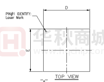
Mechanical Dimensions
Figure 4. Package Dimension
Single-Chip 802.11 a/b/g/n/ac 1T1R WLAN Controller
with USB 2.0 Interface
13
Track ID:
Rev. 0.1r05
�RTL8811CU
Datasheet
8.1. Mechanical Dimensions Notes
Symbol
A
A1
A3
b
D/E
D2
E2
e
L
Min
0.80
0.00
0.15
4.10
4.75
0.30
Dimension in mm
Nom
0.85
0.02
0.2 REF
0.20
7.00 BSC
4.20
4.85
0.40 BSC
0.40
Max
0.90
0.05
Min
0.031
0.000
0.25
0.006
4.30
4.95
0.161
0.187
0.50
0.012
Dimension in inch
Nom
0.033
0.001
0.008 REF
0.008
0.276 BSC
0.165
0.191
0.016 BSC
0.016
Max
0.035
0.002
0.010
0.169
0.195
0.020
Notes:
1. CONTROLLING DIMENSION:MILLIMETER(mm).
2. REFERENCE DOCUMENTL:JEDEC MO-220.
Table 13. Package Dimensions Notes
Single-Chip 802.11 a/b/g/n/ac 1T1R WLAN Controller
with USB 2.0 Interface
14
Track ID:
Rev. 0.1r05
�RTL8811CU
Datasheet
9.
Ordering Information
Part Number
RTL8811CU-CG
Package
QFN56 , ‘Green’ Package
Table 14.
Status
To be available
Ordering Information
Realtek Semiconductor Corp.
Headquarters
No. 2, Innovation Road II, Hsinchu Science Park,
Hsinchu 300, Taiwan, R.O.C.
Tel: 886-3-5780211 Fax: 886-3-5776047
www.realtek.com
Single-Chip 802.11 a/b/g/n/ac 1T1R WLAN Controller
with USB 2.0 Interface
15
Track ID:
Rev. 0.1r05
�