UMW
R
ST485E
Low-Power, Slew-Rate-Limited RS-485/RS-422 Transceivers
General Description
The ST485 is low-power transceivers for RS-485 and RS422 communication. IC contains one driver and one receiver.
The driver slew rates of the ST485 is not limited, allowing
them to transmit up to 2.5Mbps.
These transceivers draw between 120µA and 500µA of
supply current when unloaded or fully loaded with disabled
drivers. All parts operate from a single 5V supply. Drivers are
short-circuit current limited and are protected against
excessive power dissipation by thermal shutdown circuitry
that places the driver outputs into a high-impedance state.
The receiver input has a fail-safe feature that guarantees a
logic-high output if the input is open circuit. The ST485 is
designed for half-duplex applications.
Features
Low Quiescent Current: 300µA
-7V to +12V Common-Mode Input Voltage Range
Three-State Outputs
30ns Propagation Delays, 5ns Skew
Full-Duplex and Half-Duplex Versions Available
Operate from a Single 5V Supply
Allows up to 32 Transceivers on the Bus
Data rate: 2,5 Mbps
Current-Limiting and Thermal Shutdown for Driver Overload Protection
www.umw-ic.com
1
UTD Semiconductor Co.,Limited
�UMW
R
ST485E
Low-Power, Slew-Rate-Limited RS-485/RS-422 Transceivers
ABSOLUTE MAXIMUM RATINGS
Supply Voltage (VCC) 12V
Control Input Voltage -0.5V to (VCC + 0.5V)
Continuous Power Dissipation (TA= +70°C)
8-Pin Plastic DIP (derate 9.09mW/°C above
+70°C) 727mW
8-Pin SO (derate 5.88mW/°C above +70°C)
471mW
Operating Temperature Ranges-40°C to +85°C
Storage Temperature Range -65°C to +160°C
Lead Temperature (soldering, 10sec) +300°C
Driver Input Voltage (DI) -0.5V to (VCC+ 0.5V)
Driver Output Voltage (A, B) -8V to +12.5V
Receiver Input Voltage (A, B) -8V to +12.5V
Receiver Output Voltage (RO) -0.5V to
(VCC+0.5V)
DC ELECTRICAL CHARACTERISTICS
(VCC = 5V ±5%, TA = TMIN to TMAX, unless otherwise noted.) (Notes 1, 2)
PARAMETER
SYMBOL
Differential Driver Output (no
load)
Differential Driver Output
(with load)
Change in Magnitude of Driver
Differential Output Voltage for
Complementary Output States
Driver Common-Mode Output
Voltage
Change in Magnitude of Driver
Common-Mode Output Voltage
for Complementary Output
States
Input High Voltage
VOD1
VOD2
∆VOD
CONDITIONS
R = 50Ω (RS-422)
R = 27Ω (RS-485), Figure 4
R = 27Ω or 50Ω, Figure 4
TYP
MAX
UNITS
5
V
V
2
1.5
5
0.2
V
VOC
R = 27Ω or 50Ω, Figure 4
3
V
∆VOD
R = 27Ω or 50Ω, Figure 4
0.2
V
VIH
DE, DI, RE
Input Low Voltage
VIL
DE, DI, RE
Input Current
Input Current
(A, B)
IIN1
Receiver Differential Threshold
Voltage
Receiver Input Hysteresis
Receiver Output High Voltage
Receiver Output Low Voltage
Three-State (high impedance)
Output Current at Receiver
Receiver Input Resistance
VTH
DE, DI, RE
DE = 0V;
VCC = 0V or 5.25V,
-7V ≤ VCM ≤12V
www.umw-ic.com
MIN
IIN2
∆VTH
VOH
VOL
IOZR
RIN
2.0
0.8
VIN = 12V
VIN = -7V
VCM = 0V
IO = -4mA, VID = 200mV
IO = 4mA, VID = -200mV
0.4V ≤ VO ≤ 2.4V
-7V ≤ VCM ≤ 12V
2
V
-0.2
V
±2
µA
1.0
-0.8
0.2
mA
70
3.5
0.4
±1
V
mV
V
V
µA
kΩ
UTD Semiconductor Co.,Limited
�UMW
R
ST485E
Low-Power, Slew-Rate-Limited RS-485/RS-422 Transceivers
DC ELECTRICAL CHARACTERISTICS (continued)
(VCC = 5V ±5%, TA = TMIN to TMAX, unless otherwise noted.) (Notes 1, 2)
PARAMETER
No-Load Supply Current
(Note 3)
SYMBOL
ICC
CONDITIONS
MIN
DE = VCC
RE = 0V or VCC
TYP
MAX
UNITS
500
300
900
500
µA
DE = 0V
Driver Short-Circuit Current,
IOSD1
-7V ≤ VO ≤ 12V (Note 4)
35
250
mA
IOSD2
-7V ≤ VO ≤12V (Note 4)
35
250
mA
IOSR
0V ≤ VO ≤ VCC
7
95
mA
VO = High
Driver Short-Circuit Current,
VO = Low
Receiver Short-Circuit Current
SWITCHING CHARACTERISTICS
(VCC = 5V ±5%, TA = TMIN to TMAX, unless otherwise noted.) (Notes 1, 2)
PARAMETER
Driver Input to Output
Driver Output Skew to Output
Driver Enable to Output High
Driver Enable to Output Low
Driver Disable Time from Low
Driver Disable Time from High
| tPLH - tPHL | Differential
Receiver Skew
Receiver Enable to Output
Low
Receiver Enable to Output
High
Receiver Disable Time from
Low
Receiver Disable Time from
High
Maximum Data Rate
www.umw-ic.com
SYMBOL
CONDITIONS
MIN
TYP
MAX
UNITS
tPLH
tPHL
10
10
30
30
5
40
40
40
40
13
60
60
10
70
70
70
70
ns
tZL
RDIFF = 54Ω
CL1 = CL2 = 100pF
RDIFF = 54Ω, CL1 = CL2 = 100pF
CL= 100pF, S2 closed
CL= 100pF, S1 closed
CL= 15pF, S1 closed
CL= 15pF, S2 closed
RDIFF = 54Ω
CL1 = CL2 = 100pF
CRL = 15pF, S1 closed
20
50
ns
tZH
CRL = 15pF, S2 closed
20
50
ns
tLZ
CRL = 15pF, S1 closed
20
50
ns
tHZ
CRL = 15pF, S2 closed
20
50
ns
tSKEW
tZH
tZL
tLZ
tHZ
tSKD
fMAX
2.5
3
ns
ns
ns
ns
ns
ns
Mbps
UTD Semiconductor Co.,Limited
�UMW
R
ST485E
Low-Power, Slew-Rate-Limited RS-485/RS-422 Transceivers
Operation timing diagrams of ST485
Table of ST485 operation
RE
X
X
0
1
Transmission
Inputs
DE
DI
1
1
1
0
0
X
0
X
Outputs X
Z
Y
0
1
1
0
Z
Z
Z
Z
RE
0
0
0
1
Receipt
Inputs
DE
A-B
0
+0.2V
0
-0.2V
0
open
0
X
Outputs
RO
1
0
1
Z
X-don’t care
Z-high resistance
www.umw-ic.com
4
UTD Semiconductor Co.,Limited
�UMW
R
ST485E
Low-Power, Slew-Rate-Limited RS-485/RS-422 Transceivers
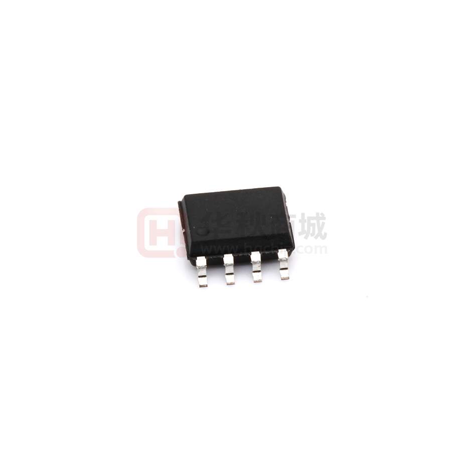
SOP-8
Symbol
A
A1
A2
b
c
D
E
E1
e
L
θ
www.umw-ic.com
Dimensions In Millimeters
Min
Max
1.350
1.750
0.100
0.250
1.350
1.550
0.330
0.510
0.170
0.250
4.700
5.100
3.800
4.000
5.800
6.200
1.270(BSC)
0.400
1.270
0°
8°
5
Dimensions In Inches
Min
Max
0.053
0.069
0.004
0.010
0.053
0.061
0.013
0.020
0.006
0.010
0.185
0.200
0.150
0.157
0.228
0.244
0.050(BSC)
0.016
0.050
0°
8°
UTD Semiconductor Co.,Limited
�UMW
R
ST485E
Low-Power, Slew-Rate-Limited RS-485/RS-422 Transceivers
Ordering information
Order code
Package
Baseqty
Deliverymode
UMW ST485EBDR
SOP-8
2500
Tape and reel
www.umw-ic.com
6
UTD Semiconductor Co.,Limited
�
