VIS30038
30V N-Channel Power Trench MOSFET
General Description
Product Summary
• Trench Power MOSFET Technology
VDS
• Low RDS(ON)
ID
(at VGS=10V)
81A
• Optimized for High Reliable Switch Application
RDS(ON)
(at VGS=10V, typ)
3.6mΩ
• High Current Capability
RDS(ON)
(at VGS=4.5V, typ)
4.8mΩ
30V
• RoHS and Halogen-Free Compliant
Applications
• Motor Drive
100% UIS Tested
• Load Switch
100% RG Tested
• Battery Protection
• General DC/DC Converters
D
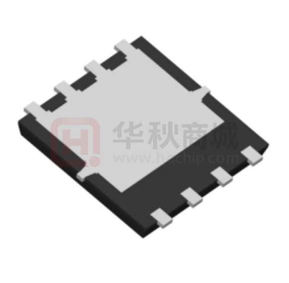
DFN5X6
Top View
S
S
S
G
G
S
Bottom View
1
8
2
7
3
6
4
5
D
D
D
PIN1
D
Orderable Part Number
Package Type
Form
Minimum Order Quantity
VIS30038
DFN5x6
Tape & Reel
5000
Absolute Maximum Ratings TA=25°C unless otherwise noted
Parameter
Symbol
Drain-Source Voltage
Gate-Source Voltage
TC=25°C
Continuous Drain
Current (5)
Pulsed Drain Current
Continuous Drain
Current
(3)
VDS
30
V
VGS
±20
V
81
A
51
A
233
A
32
A
25.6
A
33.3
IDM
TC=25°C
IDSM
TA=100°C
IAS
Avalanche Energy L=0.1mH
Power Dissipation (1)
Units
ID
TC=100°C
Avalanche Current (3)
Power Dissipation (2)
Maximum
(3)
EAS
TC=25°C
PD
TC=100°C
TC=25°C
PDSM
TA=100°C
Junction and Storage Temperature Range
TJ, TSTG
55
A
mJ
44.6
W
17.8
W
6.9
W
4.4
W
°C
-55 to 150
Thermal Characteristics
Parameter
Maximum Junction-to-Ambient
Symbol
(1)
t ≤ 10s
Maximum Junction-to-Ambient (1,4)
Steady-State
Maximum Junction-to-Case
Steady-State
Rev0.92 (03/2021)
RθJA
RθJC
Typ
Max
Units
15
18
°C/W
35
42
°C/W
2.3
2.8
°C/W
Voltaic Semiconductor Confidential and Proprietary Information
1
�VIS30038
30V N-Channel Power Trench MOSFET
Electrical Characteristics (TJ=25°C unless otherwise noted)
Symbol
Parameter
Conditions
Min
Typ
Max
Units
STATIC PARAMETERS
BVDSS
Drain-Source Breakdown Voltage
ID=250µA, VGS=0V
IDSS
Zero Gate Voltage Drain Current
IGSS
Gate-Body leakage current
VDS=0V, VGS=±20V
VGS(th)
Gate Threshold Voltage
VDS=VGS, ID=250µA
V
VDS=30V, VGS=0V
1
TJ=55°C
VGS=10V, ID=20A
RDS(ON)
30
Static Drain-Source On-Resistance
TJ=125°
VGS=4.5V, ID=20A
5
1.4
μA
±100
nA
1.8
2.2
V
3.6
4.3
5.1
4.8
mΩ
6.6
gFS
Forward Transconductance
VDS=5V, ID=20A
71
S
VSD
Diode Forward Voltage
IS=1A, VGS=0V
0.71
V
IS
Maximum Body-Diode Continuous Current
58
A
DYNAMIC PARAMETERS
Ciss
Input Capacitance
Coss
Output Capacitance
Crss
Reverse Transfer Capacitance
Rg
Gate resistance
VGS=0V, VDS=15V,
f=1MHz
f=1MHz
2366
pF
350
pF
225
pF
0.8
Ω
45.5
nC
21.6
nC
9.7
nC
SWITCHING PARAMETERS
Qg(10V)
Total Gate Charge
Qg(4.5V)
Total Gate Charge
Qgs
Gate Source Charge
Qgd
Gate Drain Charge
9.4
nC
tD(on)
Turn-On Delay Time
12.3
ns
tr
Turn-On Rise Time
tD(off)
Turn-Off Delay Time
tf
Turn-Off Fall Time
trr
Body Diode Reverse Recovery Time
IF=20A, di/dt=200A/μs
6.8
ns
Qrr
Body Diode Reverse Recovery Charge
IF=20A, di/dt=200A/μs
10.2
nC
1)
2)
3)
4)
5)
VGS=10V, VDS=15V,
ID=20A
VGS=10V, VDS=15V,
RL=0.75Ω, RGEN=3Ω
9.4
ns
28.5
ns
9.8
ns
2
RθJA is measured with the device mounted on 1in FR-4 board with 2oz. Copper, in a still air environment with TA =25°C. The Power dissipation PDSM
is based on RθJA t≤ 10s and the maximum allowed junction temperature of 150°C. The value in any given application depends on the user's specific
board design.
The power dissipation PD is based on TJ(MAX)=150°C, using junction-to-case thermal resistance, and is more useful in setting the upper dissipation
limit for cases where additional heatsinking is used.
Single pulse width limited by junction temperature TJ(MAX)=150°C.
RθJA is the sum of the thermal impedance from junction to case RθJC and case to ambient.
The maximum current rating is package limited.
Rev0.92 (03/2021)
Voltaic Semiconductor Confidential and Proprietary Information
2
�VIS30038
30V N-Channel Power Trench MOSFET
TYPICAL ELECTRICAL AND THERMAL CHARACTERISTICS
150
200
4.5V
125
7V
150
125
3.5V
10V
ID (A)
ID (A)
100
75
VDS=5V
175
100
75
50
TJ=150°C
50
3V
25
TJ=25°C
25
VGS=2.5V
0
0
0
1
2
3
4
5
0.0
1.0
2.0
VDS (V)
4.0
5.0
6.0
Fig 2. Typical Transfer Characteristics
1.6
4000
1.5
3500
1.4
Capacitance (pF)
Normalized On-Resistance
Fig 1. Typical Output Characteristics
VGS=4.5V
ID=20A
1.3
3.0
VGS (V)
1.2
1.1
VGS=10V
ID=20A
1
3000
Ciss
2500
2000
1500
Coss
Crss
1000
0.9
500
0.8
0
25
50
75
100
125
0
150
0
5
10
TJ, Junction Temperature (℃)
15
20
25
30
1
1.2
VDS (V)
Fig 3. Normalized On-Resistance vs. Temperature
Fig 4. Typical Capacitance vs. VDS
10
1000
9
8
100
TJ=150°C
6
IS(A)
VGS(V)
7
5
TJ=25°C
10
4
3
1
2
1
0
0.1
0
10
20
30
40
50
0
0.2
0.4
Qg(nC)
Fig 5. Typical Gate Charge vs. VGS
Rev0.92 (03/2021)
0.6
0.8
VSD(V)
Fig 6. Typical Source-Drain Diode Forward Voltage
Voltaic Semiconductor Confidential and Proprietary Information
3
�VIS30038
30V N-Channel Power Trench MOSFET
TYPICAL ELECTRICAL AND THERMAL CHARACTERISTICS
1000
90
100
RDS(ON)
limited
ID (A)
100μs
10
1ms
DC
10ms
1
TJ(MAX)=150℃
Current Rating ID (A)
80
10μs
70
60
50
40
30
20
10
TC=25℃
0.1
0.01
0.1
0
1
10
0
100
25
50
Fig 7. Maximum Safe Operating Area
125
150
Fig 8. Maximum Drain Current vs. Case Temperature
10
ZθJC Normalized Transient
Thermal Resistance
100
TCASE (℃)
VDS(V)
1
75
In descending order
D=0.5, 0.3, 0.1, 0.05, 0.02, 0.01, 0.005, single pulse
D=Ton/T
TJ,PK=TA+PDM∙ZθJC∙RθJC
RθJC=2.8℃/W
0.1
PD
0.01
TON
T
0.001
0.00001
0.0001
0.001
0.01
0.1
1
10
Pulse Width (s)
Fig 9. Normalized Maximum Transient Thermal Impedance, Junction-to-Case
ZθJA Normalized Transient
Thermal Resistance
10
1
In descending order
D=0.5, 0.3, 0.1, 0.05, 0.02, 0.01, 0.005, single pulse
D=Ton/T
TJ,PK=TA+PDM∙ZθJA∙RθJA
RθJA=42℃/W
0.1
PD
0.01
TON
T
0.001
0.001
0.01
0.1
1
10
100
1000
Pulse Width (s)
Fig 10. Normalized Maximum Transient Thermal Impedance, Junction-to-Ambient
Rev0.92 (03/2021)
Voltaic Semiconductor Confidential and Proprietary Information
4
�VIS30038
30V N-Channel Power Trench MOSFET
TYPICAL ELECTRICAL AND THERMAL CHARACTERISTICS
1000
10000
TJ(MAX)=150℃
800
TA=25℃
1000
Power (W)
Power (W)
TJ(MAX)=150℃
TC=25℃
600
400
100
10
200
0
0.00001 0.0001
0.001
0.01
0.1
1
1
0.00001
10
0.001
Pulse Width (s)
0.1
10
Fig 11. Single Pulse Power Rating Junction-to-Case
Fig 12. Single Pulse Power Rating Junction-to-Ambient
50
15
ID=20A
45
12.5
40
35
RDSON (mΩ)
Power Dissipation (W)
1000
Pulse Width (s)
30
25
20
15
10
7.5
150℃
5
10
2.5
5
25℃
0
0
25
50
75
100
125
150
0
2
4
TCASE (℃)
6
8
10
VGS (V)
Fig 13. Maximum Power Rating vs. Temperature
Fig 14. On-Resistance vs. VGS
8
RDSON (mΩ)
7
6
VGS=4.5V
5
4
VGS=10V
3
2
0
20
40
60
80
ID (A)
Fig 15. On-Resistance vs. Drain Current
Rev0.92 (03/2021)
Voltaic Semiconductor Confidential and Proprietary Information
5
�VIS30038
30V N-Channel Power Trench MOSFET
TEST CIRCUIT
BV DSS
VDS
L
IAS
+
VDD
DUT
IAS
Fig16. Unclamped Inductive Test Circuit
Fig17. Unclamped Inductive Waveform
VDS
Qg
VGS
10V
L
DUT
VCC
Qg s
Fig18. Qg Test Circuit
Qgd
Fig19. Qg Waveform
RL
VDS
90%
+
VGS
RG
DUT
VDD
10%
tr
td (on )
td(off)
to n
Fig18. Resistive Switching Test Circuit
Rev0.92 (03/2021)
tf
to ff
Fig19. Switching Time Waveform
Voltaic Semiconductor Confidential and Proprietary Information
6
�VIS30038
30V N-Channel Power Trench MOSFET
TEST CIRCUIT
VDS+
VG S
DUT
VDS-
L
ISD
ISD
+
VGS
VDD
IF
dI/ dt
trr
VD D
VD S
Fig20. Diode Recovery Test Circuit
Fig21. Diode Recovery Test Waveform
L1
D1
A
C
DFN5x6 OUTLINE
E4
H
D2
e
b
L
K
Rev0.92 (03/2021)
DIM
SYMBOL
A
b
C
D1
D2
e
E1
E2
E4
H
K
L
L1
MILLIMITERS
MIN [mm]
MAX [mm]
0.900
1.000
0.350
0.450
0.254 REF
4.824
4.976
3.910
4.110
1.270 TYP
5.974
6.126
5.674
5.826
3.375
3.575
0.574
0.726
1.190
1.390
0.559
0.711
0
0.120
Voltaic Semiconductor Confidential and Proprietary Information
7
�
很抱歉,暂时无法提供与“VIS30038”相匹配的价格&库存,您可以联系我们找货
免费人工找货