Jul. 2020
S C B 1 2 Q 4 G x x0 A F
4Gbit DDR4 SDRAM
E U Ro H S Co m p lia n t Pr o d u c t s
D a t a She e t
Re v . D
�Data Sheet
SCB12Q4Gxx0AF
4Gbit DDR4 SDRAM
Revision History
Date
Revision
Subjects (major changes since last revision)
2019-08
A
2019-10
B
Initial Release
Modify some type
Update Product list:
Add SCB12Q4G800AF-08T, SCB12Q4G160AF-08T
2020-05
C
2020-07
D
Update package outline of x 16 Product:Modify some typo.
Format review (2020-05-28)
Add Table 2: 4Gbit DDR4 Addressing
We Listen to Your Comments
Any information within this document that you feel is wrong, unclear or missing at all? Your feedback will help us to
continuously improve the quality of this document. Please send your proposal (including a reference to this document) to:
info@unisemicon.com
UniIC_Techdoc, Rev. D 2020-07
2 / 32
�Data Sheet
SCB12Q4Gxx0AF
4Gbit DDR4 SDRAM
Contents
Contents ........................................................................................................................................................................................ 3
1
Features .................................................................................................................................................................................. 4
2
Product List ............................................................................................................................................................................. 5
3
Ball configuration..................................................................................................................................................................... 6
4
Ball Description ....................................................................................................................................................................... 8
5
Electrical Specifications......................................................................................................................................................... 10
6
Speed Bin .............................................................................................................................................................................. 12
7
Electrical Characteristics & Timing ........................................................................................................................................ 15
7.1
Reference Load for AC Timing and Output Slew Rate ............................................................................................... 15
7.2
Timing Parameters by Speed Grade .......................................................................................................................... 16
8
Package Outlines .................................................................................................................................................................. 27
9
Product Type Nomenclature .................................................................................................................................................. 29
List of Figures .............................................................................................................................................................................. 30
List of Tables ............................................................................................................................................................................... 31
UniIC_Techdoc, Rev. D 2020-07
3 / 32
�Data Sheet
SCB12Q4Gxx0AF
4Gbit DDR4 SDRAM
1
Features
The 4Gbit DDR4 SDRAM offers the following key features:
• Operating case temperature range TC = 0℃ to +95℃
• Refresh cycles
Average refresh period 7.8s at 0℃ TC +85℃
3.9s at +85℃ < TC +95℃
• Fine granularity refresh is supported
• Adjustable internal generation VREFDQ
• Pseudo Open Drain (POD) interface for data
input/output
• Driver strength selected by MRS
• The high-speed data transfer by the 8 bits pre-fetch
• Temperature Controlled Refresh (TCR) mode
is supported
• Low Power Auto Self Refresh (LPASR) mode
is supported
• Self refresh abort is supported
• Programmable preamble is supported
• Write leveling is supported
• Command/Address latency (CAL) is supported
• Multipurpose register READ and WRITE capability
• Command Address Parity (CA Parity) for
command address signal error detect and inform
it to controller
• Write Cyclic Redundancy Code (CRC) for DQ
error detect and inform it to controller during
high-speed operation
• Data Bus Inversion (DBI) for Improve the
power consumption and signal integrity of the
memory interface
• Data mask (DM) for write data
• Per DRAM Addressability (PDA) for each DRAM
can be set a different mode register value individually
and has individual adjustment
• Gear down mode (1/2 and 1/4 rate) is supported
• PPR and sPPR is supported
• Connectivity test (x16 only)
• Maximum power down mode for the lowest
power consumption with no internal refresh activity
• JEDEC JESD-79-4 compliant
• Power supply
5%
- VPP = 2.5V – 5% + 10%
• Data rate
- 2666Mbps (DDR4-2666)
- 2400Mbps (DDR4-2400)
• Package
- 78-ball FBGA
- 96-ball FBGA
- Lead-free
• 16 or 8 internal banks
4 groups of 4 banks each (x4 and x8)
2 groups of 4 banks each (x16)
• Differential clock inputs operation
(CK_t and CK_c)
• Bi-directional differential data strobe
(DQS_t and DQS_c)
• Termination Data Strobe is supported (x8 only)
(TDQS_t and TDQS_c)
• Asynchronous reset is supported
(RESET_n)
• ZQ calibration for Output driver by compare to
external reference resistance
(RZQ 240 ohm
• Nominal, park and dynamic On-die Termination
(ODT)
• DLL aligns DQ and DQS transitions with CK
transitions
• Commands entered on each positive CK edge
• CAS Latency (CL): 9, 10, 11, 12, 13, 14, 15, 16, 17, 18,
19, 20, 21, 22 and 23 supported
• Additive Latency (AL) 0, CL-1, and CL-2 supported
• Burst Length (BL): 8 and 4 with on the fly supported
• CAS Write Latency (CWL): 9, 10, 11, 12, 14, 16 and 18
supported
UniIC_Techdoc, Rev. D 2020-07
4 / 32
�Data Sheet
SCB12Q4Gxx0AF
4Gbit DDR4 SDRAM
2
Product List
Table 1 shows all possible products within the 4Gbit DDR4 SDRAM component generation.
Table 1 - Ordering Information for 4Gbit DDR4 Component
UniIC Part Number
Max. Clock
frequency
CAS-RCD-RP
latencies
Speed Sort
Name
Package
4Gbit DDR4 SDRAM Components in × 8 Organization (512 M × 8)
SCB12Q4G800AF-07Q
1333 MHz
19-19-19
DDR4–2666V
PG-FBGA-78
SCB12Q4G800AF-08T
1200 MHz
17-17-17
DDR4–2400T
PG-FBGA-78
4Gbit DDR4 SDRAM Components in × 16 Organization (256 M × 16)
SCB12Q4G160AF-07Q
1333 MHz
19-19-19
DDR4–2666V
PG-FBGA-96
SCB12Q4G160AF-08T
1200 MHz
17-17-17
DDR4–2400T
PG-FBGA-96
Table 2 - 4Gbit DDR4 Addressing
Parameter
512Mb × 8
256Mb × 16
Number of bank groups
4
2
Bank group address
BG[1:0]
BG0
Bank count per group
4
4
Bank address in bank group
BA[1:0]
BA[1:0]
Row Address
32K (A[14:0])
32K (A[14:0])
Column Address
1K(A[9:0])
1K(A[9:0])
Page Size
1KB
2KB
UniIC_Techdoc, Rev. D 2020-07
5 / 32
Note
�Data Sheet
SCB12Q4Gxx0AF
4Gbit DDR4 SDRAM
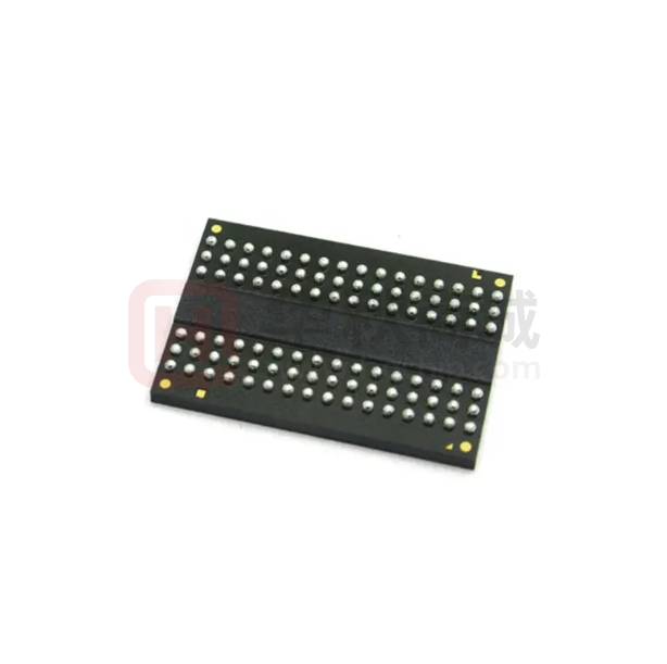
3
Ball configuration
Figure 1 - Ball out for 512Mb ×8 Components (78-ball FBGA)
UniIC_Techdoc, Rev. D 2020-07
6 / 32
�Data Sheet
SCB12Q4Gxx0AF
4Gbit DDR4 SDRAM
Figure 2 - Ball out for 256Mb ×16 Components (96-ball FBGA)
VDDQ
VSSQ
UniIC_Techdoc, Rev. D 2020-07
7 / 32
�Data Sheet
SCB12Q4Gxx0AF
4Gbit DDR4 SDRAM
4
Ball Description
Table 3 - Input / Output Signal Functional Description for 512Mb ×8 Components (78-ball FBGA)
Ball Name
Function
Address inputs
A10/AP: Auto precharge
A12/BC_n: Burst chop
Note
BA0, BA1
Bank select
2
BG0, BG1
Bank group input
2
DQ0 to DQ7
Data input/output
DQS_t, DQS_c
Differential data strobe
TDQS_t, TDQS_c
Termination data strobe
CS_n
Chip select
2
RAS_n/A16
CAS_n/A15
WE_n/A14
Command input
2
ACT_n
Activation command input
2
CKE
Clock enable
2
CK_t, CK_c
Differential clock input
DM_n
Write data mask
DBI_n
Data bus inversion
ODT
ODT control
2
RESET_n
Active low asynchronous reset
2
PAR
Command and address parity
ALERT_n
Alert
VDD
Supply voltage for internal circuit
VSS
Ground for internal circuit
VDDQ
Supply voltage for DQ circuit
VSSQ
Ground for DQ circuit
VREFCA
Reference voltage for CA
ZQ
Reference pin for ZQ calibration
NC
No connection
A0 to A14
2
1
Note:
1. Not internally connected with die.
2. Input only pins (address, command, CKE, ODT and RESET_n) do not supply termination.
UniIC_Techdoc, Rev. D 2020-07
8 / 32
�Data Sheet
SCB12Q4Gxx0AF
4Gbit DDR4 SDRAM
Table 4 - Input / Output Signal Functional Description for 256Mb ×16 Components (96-ball FBGA)
Ball Name
Function
Address inputs
A10/AP: Auto precharge
A12/BC_n: Burst chop
Note
BA0, BA1
Bank select
2
BG0
Bank group input
2
A0 to A14
DQU0 to DQU7
DQL0 to DQL7
DQSU, DQSU_n
DQSL, DQSL_n
2
Data input/output
Differential data strobe
CS_n
Chip select
2
RAS_n/A16
CAS_n/A15
WE_n/A14
Command input
2
ACT_n
Activation command input
2
CKE
Clock enable
2
CK_t, CK_c
Differential clock input
DMU_n, DML_n
Write data mask
DBIU_n, DBIL_n
Data bus inversion
ODT
ODT control
2
RESET_n
Active low asynchronous reset
2
PAR
Command and address parity
ALERT_n
Alert
TEN
Connectivity test mode enable
VDD
Supply voltage for internal circuit
VSS
Ground for internal circuit
VDDQ
Supply voltage for DQ circuit
VSSQ
Ground for DQ circuit
VREFCA
Reference voltage for CA
ZQ
Reference pin for ZQ calibration
NC
No connection
1
Note:
1. Not internally connected with die.
2. Input only pins (address, command, CKE, ODT and RESET_n) do not supply termination.
UniIC_Techdoc, Rev. D 2020-07
9 / 32
�Data Sheet
SCB12Q4Gxx0AF
4Gbit DDR4 SDRAM
5
Electrical Specifications
Table 5 - IDD & IDDQ Specification
DDR4-2400
DDR4-2666
Symbol
Unit
x8
x16
x8
x16
IDD0
79
86
85
92
mA
IDD0A
80
87
86
93
mA
IDD1
93
128
115
142
mA
IDD1A
96
122
107
146
mA
IDD2N
67
67
74
74
mA
IDD2NA
68
68
75
75
mA
IDD2NT
80
86
90
97
mA
IDD2NL
59
59
63
63
mA
IDD2NG
65
65
71
71
mA
IDD2ND
49
49
52
52
mA
IDD2N_par
82
82
94
94
mA
IDD2P
40
40
44
44
mA
IDD2Q
66
67
74
75
mA
IDD3N
78
78
86
86
mA
IDD3NA
79
79
85
85
mA
IDD3P
64
64
67
67
mA
IDD4R
150
188
165
205
mA
IDD4RA
152
197
183
227
mA
IDD4RB
149
190
166
206
mA
IDD4W
162
211
180
230
mA
IDD4WA
170
227
197
266
mA
IDD4WB
155
199
172
215
mA
IDD4WC
151
194
168
210
mA
IDD4W_par
176
215
189
204
mA
IDD5B
170
170
180
180
mA
IDD5F2
179
179
189
189
mA
IDD5F4
147
147
160
160
mA
IDD7
187
234
196
235
mA
IDD8
30
30
30
30
mA
UniIC_Techdoc, Rev. D 2020-07
10 / 32
�Data Sheet
SCB12Q4Gxx0AF
4Gbit DDR4 SDRAM
Table 6 - IPP Specification
DDR4-2400
DDR4-2666
Symbol
Unit
X8
X16
X8
X16
IPP0
4
8
5
9
mA
IPP1
4
8
5
9
mA
IPP2N
3
6
4
7
mA
IPP2P
3
6
4
7
mA
IPP3N
3
6
4
7
mA
IPP3P
3
6
4
7
mA
IPP4R
3
6
4
7
mA
IPP4W
3
6
4
7
mA
IPP5B
22
24
25
27
mA
IPP5F2
23
25
27
29
mA
IPP5F4
17
18
20
20
mA
IPP7
22
33
29
40
mA
IPP8
2
2
3
3
mA
Table 7 - IDD6 Specification
Symbol
Temperature
Range
IDD6N
DDR4-2666
DDR4-2400
Unit
Notes
IDD(max)
IPP(max)
IDD(max)
IPP(max)
0 - 85 oC
30
6
30
6
mA
1
IDD6E
0 - 95 oC
36
8
36
8
mA
2
IDD6R
0 - 45 oC
25
4
25
4
mA
3
IDD6A
0 - 85 oC
30
6
30
6
mA
4
Note:
1. Applicable for MR2 settings A6 = 0 and A7 = 0.
2. Applicable for MR2 settings A6 = 0 and A7 = 1. IDD6E is only specified for devices which support the extended temperature range feature.
3. Applicable for MR2 settings A6 = 1 and A7 = 0. IDD6R is only specified for devices which support the reduced temperature range feature.
4. Applicable for MR2 settings A6 = 1 and A7 = 1. IDD6A is only specified for devices which support the auto self-refresh feature.
UniIC_Techdoc, Rev. D 2020-07
11 / 32
�Data Sheet
SCB12Q4Gxx0AF
4Gbit DDR4 SDRAM
6
Speed Bin
Table 8 - DDR4-2400 Speed Bins
Speed Bin
DDR4-2400R
CL-nRCD-nRP
Parameter
16-16-16
Symbol
Internal read command to first
data
tAA
Internal read command to first
data with read DBI enabled
tAA_DBI
ACT to internal read or
write delay time
PRE command period
ACT to PRE command
period
ACT
to ACT
command period
or
CL = 9
max
min
max
13.32
18.00
14.1614
(13.75)5,12
18.00
tAA(min)
+ 3nCK
13.32
14.16
(13.75)5,12
-
ns
12
9 x tREFI
ns
12
-
ns
12
ns
1,2,3,4,11
32
9 x tREFI
CWL
32
46.16
(45.75)5,12
45.32
1.5
tCK(AVG)
1.6
(Optional)
Reserved
5,12
CL = 10 CL = 12
tCK(AVG)
Reserv
ed
1.5
1.6
Reserved
1.25
CL = 11 CL = 13
tCK(AVG)
CL =
tCK(AVG)
CL = 14
tCK(AVG)
CL = 13 CL = 15
tCK(AVG)
CL =
tCK(AVG)
1.25