KJ3400S
N-Channel Enhancement Mode MOSFET
1. Product Information
1.1
Features
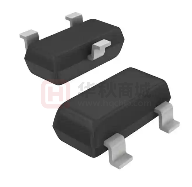
Surface-mounted package
1.2
Advanced trench cell design
Applications
Portable appliances
High speed switch
1.3
Battery management
Low power DC to DC Converter
Quick reference
RDS(ON) ≦ 26 mΩ @ VGS = 10 V
RDS(ON) ≦ 30 mΩ @ VGS = 4.5 V
RDS(ON) ≦ 45 mΩ @ VGS = 2.5 V
BV ≧ 30 V
Ptot ≦ 0.72 W
ID ≦ 5 A
2. Pin Description
Pin
Description
1
Gate (G)
2
3
Source (S)
Drain (D)
Simplified Outline
Symbol
D
3
G
1
2
Top View
SOT23
www.kjx-tech.cn
1
S
Version 0.3
�KJ3400S
3. Limiting Values
Symbol
Parameter
Conditions
Min
Max
Unit
VDS
Drain-Source Voltage
TA = 25℃
30
-
V
VGS
Gate-Source Voltage
TA = 25℃
-
±12
V
ID*
Drain Current
TA = 25℃, VGS = 10 V
-
5.0
A
Pulsed Drain Current
TA = 25℃, VGS = 10 V
-
20
A
Ptot
Total Power Dissipation
TA = 25℃
-
0.72
W
Tstg
Storage Temperature
-55
150
℃
TJ
Junction Temperature
-
150
℃
IS
Diode Forward Current
-
5.0
A
-
140
℃/W
IDM*,**
RθJA*
TA = 25 ℃
Thermal Resistance-Junction to Ambient
Notes:
*
Surface Mounted on 1 in2 pad area, t 10 sec
**
Pulse width 300 s, duty cycle 2%
4. Marking Information
Product Name
Marking
KJ3400S
3400
5. Ordering Code
Product Name
Package
KJ3400S
SOT23
Note:
Reel Size
Tape width
Quantity
Note
3000
KUAIJIEXIN defines “Green” as lead-free (RoHS compliant) and halogen free (Br or Cl does not exceed
900 ppm by weight in homogeneous material and total of Br and Cl does not exceed 1500 ppm by weight;
Follow IEC 61249-2-21 and IPC/JEDEC J-STD-020C)
www.kjx-tech.cn
2
Version 0.3
�KJ3400S
6. Electrical Characteristics (TA=25°C Unless Otherwise Noted)
Symbol
Parameter
Conditions
Min
Typ Max Unit
Static Characteristics
BVDSS
Drain-Source Breakdown Voltage
VGS = 0 V, IDS = 250 μA
30
-
-
V
VGS(th)
Gate Threshold Voltage
VDS = VGS, IDS = 250 μA
0.5
0.9
1.5
V
-
-
1
μA
IDSS
Drain Leakage Current
-
-
30
μA
VGS = ±12 V, VDS = 0 V
-
-
±100
nA
VGS = 10 V, IDS = 5 A
-
21
26
VGS = 4.5 V, IDS = 4.5 A
-
25
30
VGS = 2.5 V, IDS = 4.0 A
-
35
45
-
630
-
-
76
-
VDS = 24 V, VGS = 0 V
TJ = 85℃
IGSS
Gate Leakage Current
RDS(ON)a
On-State Resistance
Dynamic
Characteristicsb
Ciss
Input Capacitance
Coss
Output Capacitance
Crss
Reverse Transfer Capacitance
-
55
-
td(on)
Turn-on Delay Time
-
3
-
tr
Turn-on Rise Time
-
25
-
td(off)
Turn-off Delay Time
-
25
-
-
4
-
-
6
-
-
1.3
-
-
1.8
-
-
0.72 1.12
tf
VGS = 0 V, VDS = 15 V
Frequency = 1 MHz
VDS = 15 V, VGEN = 10 V,
RG = 3 Ω, RL = 2.6 Ω
Turn-off Fall Time
mΩ
pF
ns
Gate Charge Characteristicsb
Qg
Total Gate Charge
Qgs
Gate-Source Charge
Qgd
Gate-Drain Charge
VGS = 4.5 V, VDS = 15 V,
IDS = 5 A
nC
Diode Characteristics
VSDa
Diode Forward Voltage
ISD = 1A, VGS = 0 V
V
Notes: a: Pulse test ; pulse width 300 s, duty cycle 2%
b: Guaranteed by design, not subject to production testing
www.kjx-tech.cn
3
Version 0.3
�KJ3400S
7. Typical Characteristics
Current Capability
0.9
5.5
0.8
5.0
0.7
4.5
ID - Drain Current (A)
Ptot - Power (W)
Power Capability
0.6
0.5
0.4
0.3
0.2
4.0
3.5
3.0
2.5
2.0
1.5
0.1
T =25 oC
0.0
A
1.0
40
20
0
80
60
100 120 140 160
Normalized Transient Thermal Resistance
ID - Drain Current (A)
10
100us
300us
1ms
10ms
100ms
1s
DC
o
T =25 C
A
0.01
0.01
0.1
1
10
100 300
60
40
100 120 140 160
80
2
1
Duty = 0.5
0.2
0.1
0.1
0.05
0.02
0.01
0.01
Single Pulse
2
1E-3
1E-4
Mounted on 1in pad
o
R JA : 150 C/W
1E-3
0.01
0.1
1
10 30
Square Wave Pulse Duration (sec)
VDS - Drain-Source Voltage (V)
www.kjx-tech.cn
20
Transient Thermal Impedance
Safe Operation Area
30
0.1
A
0
Tmp – Mounting Point Temp. (℃)
Tmp – Mounting Point Temp. (℃)
1
T =25 oC,V G=10V
4
Version 0.3
�KJ3400S
7. Typical Characteristics (Cont.)
Normalized On Resistance
Diode Forward Current
2.0
20
VGS = 10V
1.8
I
= 4A
1.6
IS - Source Current (A)
Normalized On Resistance
DS
1.4
1.2
1.0
0.8
0.6
0.4
0.2
10
o
T =150 C
j
o
T =25 C
j
o
R @T =25 C: 25m
ON
0.0
-50 -25
0
25
50
j
1
0.0
75 100 125 150
Tj - Junction Temperature (℃)
0.2
0.4
1.0
1.2
1.4
Gate Charge
1400
10
VDS= 15V
Frequency=1MHz
I = 4A
VGS - Gate-Source Voltage (V)
1200
Ciss
C - Capacitance (pF)
0.8
VSD - Source-Drain Voltage (V)
Capacitance
1000
800
600
400
Coss
200
0
0.6
Crss
0
5
10
15
6
4
2
0
20
VDS - Drain-Source Voltage (V)
www.kjx-tech.cn
DS
8
0
2
4
6
8
10
QG - Gate Charge (nC)
5
Version 0.3
�KJ3400S
8. Typical Characteristics (Cont.)
Normalized On Resistance
Diode Forward Current
2.0
20
VGS = 10V
1.8
I
= 4A
1.6
IS - Source Current (A)
Normalized On Resistance
DS
1.4
1.2
1.0
0.8
0.6
0.4
0.2
10
o
T =150 C
j
o
T =25 C
j
o
R @T =25 C: 25m
ON
0.0
-50 -25
0
25
50
j
1
0.0
75 100 125 150
Tj - Junction Temperature (℃)
0.2
0.4
1.0
1.2
1.4
Gate Charge
Capacitance
10
VDS= 15V
Frequency=1MHz
I = 4A
VGS - Gate-Source Voltage (V)
1200
Ciss
C - Capacitance (pF)
0.8
VSD - Source-Drain Voltage (V)
1400
1000
800
600
400
Coss
200
0
0.6
Crss
0
5
10
15
8
6
4
2
0
20
VDS - Drain-Source Voltage (V)
www.kjx-tech.cn
DS
0
2
4
6
8
10
QG - Gate Charge (nC)
6
Version 0.3
�KJ3400S
8. Package Dimensions
SOT23 Package
D
0.25
L
E
E1
L1
b
e
Symbol
A
A1
A2
b
c
D
E
E1
e
e1
L
L1
θ
www.kjx-tech.cn
Dimensions In Millimeters
Min
Max
0.90
1.15
0
0.10
0.90
1.05
0.30
0.50
0.08
0.15
2.80
3.00
1.20
1.40
2.25
2.55
0.95 TYP
1.80
2.00
0.55 REF
0.30
0.50
0°
8°
7
A
A2
A1
e1
Dimensions In Inches
Min
Max
0.035
0.045
0
0.004
0.035
0.041
0.012
0.020
0.003
0.006
0.110
0.118
0.047
0.055
0.089
0.100
0.037 TYP
0.071
0.079
0.022 REF
0.012
0.020
0°
8°
Version 0.3
�
很抱歉,暂时无法提供与“KJ3400S”相匹配的价格&库存,您可以联系我们找货
免费人工找货