Application Note: SM80591E
High Efficiency, 1.5MHz, 1A
Synchronous Step Down Regulator
`
General Description
Features
The SM80591E is a high efficiency 1.5MHz
synchronous step down DC/DC regulator capable of
delivering up to 1A output current. It can operate over
a wide input voltage range from 2.5V to 5.5V and
integrates main switch and synchronous switch with
very low RDS(ON) to minimize the conduction loss.
The low output voltage ripple, the small external
inductor and the capacitor sizes are achieved with
1.5MHz switching frequency.
Ordering Information
SM80591 □(□□□ )
Applications
Package Code
Optional Spec Code
Ordering Number
SM80591EIKD
2.5V to 5.5V Input Voltage Range
Low RDS(ON) for Internal Switches (Top/Bottom)
170mΩ /100mΩ
High Switching Frequency 1.5MHz Minimizes
the External Components
Internal Soft-start Limits the Inrush Current
100% Dropout Operation
Reliable Short Circuit Protection
Output Auto Discharge Function
RoHS Compliant and Halogen Free
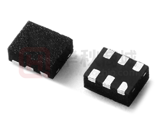
Compact Package: DFN1.1×0.9-6
Package type
DFN1.1×0.9-6
Note
--
Set Top Box
USB Dongle
Media Player
Smart phone
Typical Applications
L1:2.2µH
VIN : 2.5-5.5V
CIN
10μF/6.3V
RP G
100k
RH
100k
PG
COUT
Cff
22pF 10μF/6.3V
FB
Efficiency vs. Output Current
(IOUT=0~1A, L=2.2µH/0420CDMCCDS-2R2MC)
100
RL
49.9k
EN
ON/ OFF
VOUT :1.8V
LX
VIN
90
80
Efficiency (%)
GND
Figure1. Schematic Diagram
70
60
50
40
30
VIN =3.3V, VOUT =1.8V
VIN =4.2V, VOUT =1.8V
VIN =5.0V, VOUT =1.8V
20
Inductor and COUT Selection Table
VOUT
[V]
1.2
1.8
3.3
L
[µH]
1.5
2.2
1.5
2.2
2.2
4.7
COUT [µF]
10
√
☆
√
☆
☆
10
0
22
√
√
√
√
√
0.001
0.01
0.1
Output Current (A)
Figure2. Efficiency vs. Output Current
Note: ‘☆’ means recommended for most applications.
AN_SM80591E Rev. 0.9
© 2021 Silergy Corp.
Silergy Corp. Confidential- Prepared for Customer Use Only
1
All Rights Reserved.
1
�SM80591E
Pinout (Top View)
LX
1
6
VIN
EN
2
5
GND
PG
3
4
FB
(DFN1.1×0.9-6)
Top Mark: dxyz (device code: d, x=year code, y=week code, z= lot number code)
Pin Name
Pin Number
Pin Description
LX
1
Inductor pin. Connect this pin to the switching node of the inductor.
EN
2
Enable control. Pull high to turn on. Do not leave it floating.
PG
3
FB
4
GND
5
Ground pin.
VIN
6
Input pin. Decouple this pin to the GND pin with at least a 10µF ceramic capacitor.
Power good indicator (open drain output). Low if the output < 90% or the
output >120% of regulation voltage; High otherwise. Connect a pull-up resistor to the
input.
Output feedback pin. Connect this pin to the center point of the output resistor divider
(as shown in Figure 1) to program the output voltage: V OUT=0.6×(1+RH/RL).
Absolute Maximum Ratings (Note 1)
Supply Input Voltage------------------------------------------------------------------------------------------------- -0.3V to 6.0V
EN, FB, PG Voltage------------------------------------------------------------------------------------------ -0.3V to VIN + 0.6V
LX Voltage----------------------------------------------------------------------------------------- -0.3V (*1) to 6.0V (*2) (*3)
Power Dissipation, P D @ TA = 25°C ------------------------------------------------------------------------------- 1W
Package Thermal Resistance (Note 2)
θ JA --------------------------------------------------------------------------------------------------------------- 100°C/W
θ JC ----------------------------------------------------------------------------------------- ------------------------ 25°C/W
Junction Temperature Range ------------------------------------------------------------------------------------ -40oC to 150°C
Lead Temperature (Soldering, 10 sec.) --------------------------------------------------------------------------------- 260°C
Storage Temperature Range ----------------------------------------------------------------------------------- -65°C to 150°C
(*1)
LX Voltage Tested Down to -3V
很抱歉,暂时无法提供与“SM80591EIKD”相匹配的价格&库存,您可以联系我们找货
免费人工找货