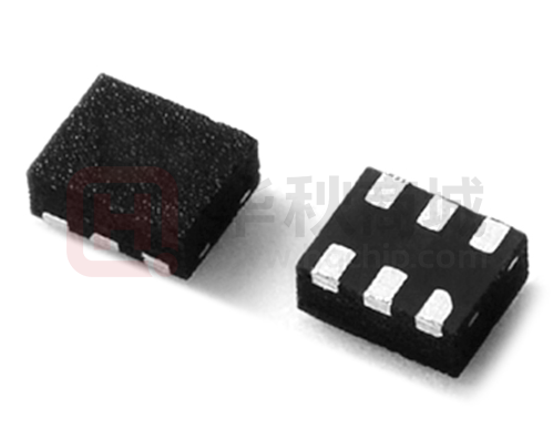
0
登录后你可以
  • 下载海量资料
  • 学习在线课程
  • 观看技术视频
  • 写文章/发帖/加入社区
创作中心
发布
  • 发文章

  • 发资料

  • 发帖

  • 提问

  • 发视频

创作活动
SM80591IKD

SM80591IKD

  • 厂商:

    SILERGY(矽力杰)

  • 封装:

    DFN6_1.2X1MM

  • 描述:

    高效1.5MHz 5.5V/1A同步降压稳压器

  • 数据手册
  • 价格&库存
SM80591IKD 数据手册
Application Note: SM80591 High Efficiency, 1.5MHz 5.5V/1A Synchronous Step Down Regulator General Description Features The SM80591 is a high efficiency 1.5MHz synchronous step down DC/DC regulator, capable of delivering up to 1A output current. It can operate over a wide input voltage range from 2.5V to 5.5V and integrate main switch and synchronous switch with very low RDS (ON) to minimize the conduction loss. The SM80591 is in a space saving, low profile DFN1.1×0.9-6 package. Ordering Information SM80591 □(□□□ ) Optional Spec Code Package type DFN1.1×0.9-6 2.5V to 5.5V Input Voltage Range 55μA Low Quiescent Current Low RDS(ON) for Internal Switches (Top/Bottom): 170mΩ /100mΩ High Switching Frequency 1.5MHz Minimizes the External Components Internal Soft-start Limits the Inrush Current 100% Dropout Operation Power Good Indicator Hic-cup for Short Circuit Protection Output Auto Discharge Function RoHS Compliant and Halogen Free Compact Package: DFN1.1×0.9-6         Applications Package Code Ordering Number SM80591IKD    Note --  Set Top Box  USB Dongle  Media Player  Smart Phone Typical Application Efficiency vs. Output Current CIN 10μF/6.3V VIN LX PG FB RH 100k RPG 100k ON/ OFF 100 COUT Cff 22pF 10μF/6.3V 90 RL 49.9k EN (IOUT=0~1A, L=2.2μH/0420CDMCCDS-2R2MC) VOUT:1.8V GND Figure1. Schematic Diagram Efficiency (%) L1:2.2µH VIN: 2.5-5.5V 80 VIN =3.3V,VOUT=1.8V 70 VIN =4.2V,VOUT=1.8V VIN =5.0V,VOUT=1.8V Inductor and COUT Selection Table VOUT [V] L[μH] 1.2/1.8/3.3 1.5 2.2 10 √ ☆ COUT [μF] 22 2×22 √ √ √ √ 60 0.001 0.01 0.1 1 Output Current (A) Figure2. Efficiency vs. Output Current Note: ‘☆ ’ means recommended for most applications. AN_SM80591 Rev. 0.0 © 2020 Silergy Corp. Silergy Corp. Confidential- Prepared for Customer Use Only 1 All Rights Reserved. SM80591 Pin out (Top View) LX 1 6 VIN EN 2 5 GND PG 3 4 FB (DFN1.1×0.9-6) Top Mark: mxyz (device code: m, x=year code, y=week code, z= lot number code) Pin Description Pin Name Pin Number Pin Description LX 1 Inductor pin. Connect this pin to the switching node of the inductor. EN 2 Enable control. Pull high to turn on. Do not leave it floating. PG 3 FB 4 GND 5 Ground pin. VIN 6 Input pin. Decouple this pin to the GND pin with at least a 10µF ceramic capacitor. Power good indicator. Power good indicator (open drain output). Low if the output < 90% or the output >120% of regulation voltage; High otherwise. Connect a pull-up resistor to the input. Output feedback pin. Connect this pin to the center point of the output resistor divider (as shown in Figure 1) to program the output voltage: V OUT=0.6×(1+RH/RL). Function Block IN Internal Power Current Sense Input UVLO EN LX 1.2V 0.6V FB OVP 120%VREF Control Logic Soft Start GND Thermal Detect PG Figure3. Block Diagram AN_SM80591 Rev. 0.0 © 2020 Silergy Corp. Silergy Corp. Confidential- Prepared for Customer Use Only 2 All Rights Reserved. SM80591 Absolute Maximum Ratings (Note 1) Supply Input Voltage----------------------------------------------------------------------------------------------- -0.3V to 6.0V FB, EN, PG Voltage----------------------------------------------------------------------------------------- -0.3V to VIN + 0.6V LX Voltage----------------------------------------------------------------------------------------- -0.3V (*1) to 6.0V (*2) Power Dissipation, PD @ TA = 25°C ------------------------------------------------------------------------------------------- 1W Package Thermal Resistance (Note 2) θ JA -------------------------------------------------------------------------------------------- ------------------- 100°C/W θ JC ----------------------------------------------------------------------------------------------------------------- 25°C/W Junction Temperature Range ------------------------------------------------------------------------------------- -40°C to 150°C Lead Temperature (Soldering, 10 sec.) --------------------------------------------------------------------------------- 260°C Storage Temperature Range ----------------------------------------------------------------------------------- -65°C to 150°C (*1) LX Voltage Tested Down to -3V
SM80591IKD 价格&库存

很抱歉,暂时无法提供与“SM80591IKD”相匹配的价格&库存,您可以联系我们找货

免费人工找货