Application Note: SQ24301
Super Low Dropout 1A LDO Regulator
Advanced Design Specification
General Description
Features
The SQ24301 is a super low dropout LDO regulator
with small package, capable of delivering up to 1A
output current.
Ordering Information
SQ24301 □(□□ □)
Package Code
Optional Spec Code
Ordering Number
SQ24301DSD
Package type
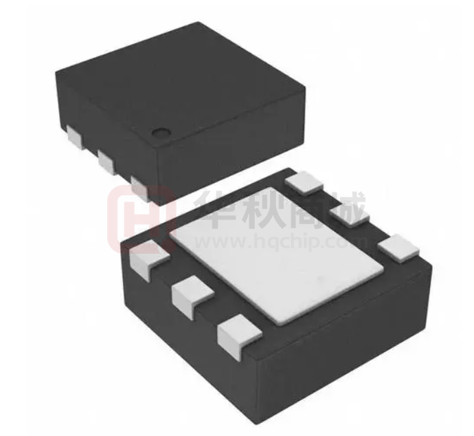
DFN3×3-6
Note
----
Input Voltage Range: 1.6-5.5V
Output Voltage Accuracy: ±5%
Up to 1A Output Current
Low Dropout Voltage:
Typ. 0.32V at IOUT=1A, VOUT=1.5V
Typ. 0.18V at IOUT=1A, VOUT=2.8V
Current Limiting Protection
Thermal Shutdown Protection
Quiescent Current: 60μA
Output Auto-discharge Function
Over Temperature Protection
RoHS Compliant and Halogen Free
Compact Package: DFN3×3-6
Applications
Portable Communication Equipments
Hand-Held Instruments, Notebook PC
Camcorders and Cameras
Typical Applications
VOUT
VIN:1.6V~5.5V
CIN
4.7µF
OUT
VIN
K
SQ24301
EN
RH
COUT
4.7µF
ADJ
RL
GND
Figure1. Schematic Diagram
AN_SQ24301 Rev. 0.0
© 2021 Silergy Corp.
Silergy Corp. Confidential- Prepared for Customer Use Only
1
All Rights Reserved.
�SQ24301
Pinout (top view)
OUT 1
OUT 2
ADJ
6 VIN
Exposed
thermal
pad
3
5
EN
4 GND
(DFN3×3-6)
Top mark: 8Txyz for SQ24301DSD (Device code: 8T, x=year code, y=week code, z= lot number code)
Pin Name
Pin Number
OUT
1, 2
ADJ
3
GND
EN
4
5
VIN
6
Pin Description
Output pin. Decouple this pin to the GND pin with at least a 4.7μF ceramic
capacitor.
Output voltage programming pin. Connect this pin to the center point of the
output resistor divider (as shown in Figure 1) to program the output voltage:
VOUT=1.0V×(1+RH/RL).
Ground pin.
Enable control pin. A 5MΩ pull-down resistor is integrated.
Input pin. Decouple this pin to the GND pin with at least a 4.7μF ceramic
capacitor.
Block Diagram
OUT
IN
ADJ
Current
limiting
Sensor
+ Ref
EN
1.0
Control
Logic
Thermal
Sensor
GND
Figure2. Block Diagram
AN_SQ24301 Rev. 0.0
© 2021 Silergy Corp.
Silergy Corp. Confidential- Prepared for Customer Use Only
2
All Rights Reserved.
�SQ24301
Absolute Maximum Ratings (Note 1)
IN, EN ------------------------------------------------------------------------------------------------------------------------- 6.0V
Power Dissipation, PD @ TA = 25°C DFN3×3-6 -------------------------------------------------------------------------- 2W
Package Thermal Resistance (Note 2)
θ JA -------------------------------------------------------------------------------------------------------------- 50°C/W
θ JC -------------------------------------------------------------------------------------------------------------- 15°C/W
Junction Temperature Range --------------------------------------------------------------------------------------------- 150°C
Lead Temperature (Soldering, 10 sec.) ---------------------------------------------------------------------------------- 260°C
Storage Temperature Range ----------------------------------------------------------------------------------- -65°C to 150°C
Recommended Operating Conditions (Note 3)
Supply Input Voltage ---------------------------------------------------------------------------------------------- 1.6V to 5.5V
Junction Temperature Range ---------------------------------------------------------------------------------- -40°C to 125°C
Ambient Temperature Range ----------------------------------------------------------------------------------- -40°C to 85°C
Electrical Characteristics
(VIN = 5V, CIN=4.7μF, COUT=4.7μF. TJ = -40°C to +125°C. Typical values are
specified. The values are guaranteed by test, design or statistical correlation.)
Parameter
Symbol
Test Conditions
Input Voltage Range
VIN
Supply Current
ISS
VEN=VIN=2V, VOUT=VADJ, IOUT=0A
Shutdown Current
ISD
VIN=6.0V, VEN=0
Output Voltage
VOUT=VADJ, VIN=2.0V,
△ VOUT
Accuracy
IOUT=100mA
Output Voltage Range
Current Limit
ILIM
VOUT=VADJ, VIN=2.0V
Load Regulation
△ VOUT/△ IOUT
1mA≤IOUT≤1A
△ VOUT/
VOUT=VADJ, IOUT=100mA
Line Regulation
△ VIN
2.0≤VIN≤5.5V
EN Pull-down
REN
Resistance
f=1kHz, Ripple 0.5VP-P
Ripple Rejection
RR
VOUT=VADJ, VIN=2.5V,
IOUT=100mA
Output Voltage
IOUT=100mA
Temperature
△ VOUT/△ T
-40℃≤TJ≤85℃
Coefficient
Short Current Limit
ISHORT
VOUT=0V
Discharge Resistor
RDISCHG
EN Rising Threshold
VENH
EN Falling Threshold
VENL
Thermal Shutdown
TSD
Temperature (Note 4)
Thermal Shutdown
THYS
Hysteresis (Note 4)
Dropout Voltage
VDROP
Refer to following table
AN_SQ24301 Rev. 0.0
© 2021 Silergy Corp.
at TJ = 25°C, unless otherwise
Min
1.6
Typ.
Max
5.5
100
10
Unit
V
µA
µA
0.95
1.05
V
1.0
1.0
VIN
V
A
60
0.1
-3
0.05
mV/A
0.3
%/V
5
MΩ
-60
dB
±100
ppm/°C
250
100
mA
Ω
V
V
1.0
0.3
150
°C
20
°C
Silergy Corp. Confidential- Prepared for Customer Use Only
3
All Rights Reserved.
�SQ24301
Dropout Voltage by output Voltage
Output Voltage(V)
VOUT
1.0V≤VOUT < 1.5V
1.5V≤ VOUT < 2.6V (Note 4)
2.6V≤VOUT (Note 4)
Typ.
0.18
0.10
0.05
TJ = -40°C to +125°C.
Dropout Voltage VDROP (V)
I=300mA
I=1A
Max
Typ
0.32
0.50
0.15
0.28
0.10
0.18
Note 1: Stresses beyond the “Absolute Maximum Ratings” may cause permanent damage to the device. These are
stress ratings only. Functional operation of the device at these or any other conditions beyond those indicated in the
operational sections of the specification is not implied. Exposure to absolute maximum rating conditions for
extended periods may affect device reliability.
Note 2:
θ JA is measured in the natural convection at TA = 25°C on a two-layer Silergy evaluation board.
Note 3: The device is not guaranteed to function outside its operating conditions.
Note 4: Guaranteed by design.
AN_SQ24301 Rev. 0.0
© 2021 Silergy Corp.
Silergy Corp. Confidential- Prepared for Customer Use Only
4
All Rights Reserved.
�SQ24301
Typical Operating Characteristics
Load Regulation
Dropout Voltage vs. Input Voltage
(VIN=2V, CIN=4.7μF, COUT=4.7μF)
1.010
0.6
IOUT=0.3A
IOUT=1.0A
Output Voltage (V)
Dropout Voltage (V)
0.5
0.4
0.3
0.2
1.005
1.000
0.995
0.1
0
1.0
0.990
1.2
1.4
1.6
1.8
2.0
2.2
2.4
2.6
2.8
3.0
0
0.1
0.2
0.3
0.4
0.5
0.6
0.7
0.8
0.9
1
Load Current (A)
Input Voltage (V)
Line Regulation
Power Supply Rejection Ratio
(IO=0.1A, CIN=4.7μF, COUT=4.7μF)
(VIN=2.5V, Io=0.1A, CIN=4.7μF, COUT=4.7μF)
1.010
10
-10
Gain(dB)
Output Voltage (V)
0
1.005
1.000
0.995
-20
-30
-40
-50
-60
0.990
1.5
2
2.5
3
3.5
4
4.5
5
Input Voltage (V)
5.5
-70
1k
10k
100k
Startup from EN
Shutdown from EN
(VIN=2V, VOUT=1V, IO=1A)
(VIN=2V, VOUT=1V, IO=1A)
VEN
2.0V/div
VOUT
1.0V/div
IOUT
VEN
2.0V/div
VOUT
1.0V/div
500mA/div
IOUT
Time (20μs/div)
AN_SQ24301 Rev. 0.0
© 2021 Silergy Corp.
500k
Frequency (Hz)
500mA/div
Time (10μs/div)
Silergy Corp. Confidential- Prepared for Customer Use Only
5
All Rights Reserved.
�SQ24301
Load Transient
Short Circuit Protection
(VIN=2V, VOUT=1V, IO=0.1~1A)
(VIN=2V, VOUT=1V, 1A to hard short)
VOUT 500mV/div
∆VOUT
IOUT
200mV/div
500mA/div
Time (40μs/div)
AN_SQ24301 Rev. 0.0
© 2021 Silergy Corp.
IOUT
500mA/div
Time (2ms/div)
Silergy Corp. Confidential- Prepared for Customer Use Only
6
All Rights Reserved.
�SQ24301
Operation Information
For better accuracy, choosing RL
很抱歉,暂时无法提供与“SQ24301DSD”相匹配的价格&库存,您可以联系我们找货
免费人工找货