Application Note: SQ25202
High Efficiency 1MHz, 2A Step Up Regulator
General Description
Features
The SQ25202 is a high efficiency, current-mode
control Boost DC to DC regulator with an integrated
200mΩ RDS(ON) N-channel MOSFET. The fixed 1MHz
switching frequency and internal compensation reduce
external component count and save the PCB space. The
build-in internal soft start circuitry minimizes the
inrush current at start-up.
•
•
•
•
•
•
•
•
RO
N
IR
IT
Ordering Information
Wide Input Range: 3-30V Bias Input, 33VOUT, MAX
1MHz Switching Frequency
Minimum ON Time: 100ns typical
Minimum OFF Time: 100ns typical
Low RDS(ON): 200mΩ
RoHS Compliant and Halogen Free
Accurate Reference: 0.6VREF
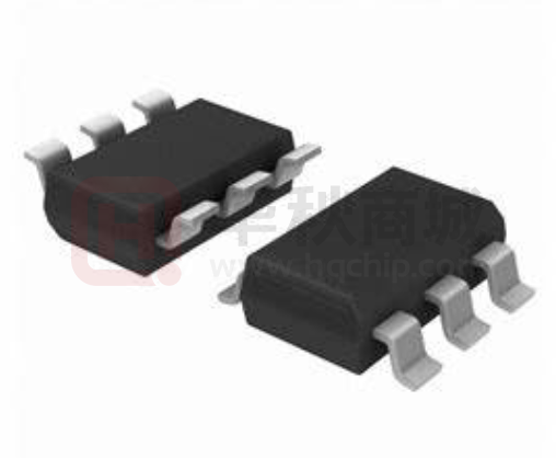
Compact Package: SOT23-6
Note
----
Typical Applications
L1 4.7uH
ON/ OFF
4
1
IN
COUT
10uFх2
LX
NC SQ25202
EN
FB
3
R1
200k
GND
VIN=5V,VOUT=12V
94
Efficiency (%)
6
de
nti
a
5
on
fi
CIN
10uF
Efficiency vs. Input Voltage
VOUT 12V
lP
VIN 5V
• Digital Camera
• Cell Phone
• PDA, PMP, MP3
dF
Package type
SOT23-6
rep
are
Ordering Number
SQ25202ABC
or
K
Applications
92
90
88
86
.C
2
R2
10.5k
orp
R3
1M
0
0.1
0.2
0.3
0.4
0.5
Load Current (A)
Figure 2. Efficiency vs. Load Current
Sil
erg
yC
Figure1. Schematic Diagram
84
AN_SQ25202 Rev.0.9
© 2022 Silergy Corp.
Silergy Corp. Confidential- Prepared for Customer Use Only
1
All Rights Reserved.
�SQ25202
LX
1
6
NC
GND 2
5
IN
FB
4
EN
3
RO
N
Pinout (top view)
IR
IT
(SOT23-6)
FB
3
EN
IN
NC
4
5
6
Pin Description
Inductor node. Connect an inductor between the IN pin and the LX pin.
Ground pin.
Feedback pin. Connect a resistor R1 between VOUT and FB, and a resistor R2 between FB
and GND to program the output voltage: VOUT=0.6V×(R1/R2+1).
Enable control. High to turn on the part. Don’t leave it floating.
Input pin. Decouple this pin to the GND pin with a 1μF ceramic capacitor.
No connection.
dF
Pin
Number
1
2
rep
are
Pin
Name
LX
GND
or
K
Top Mark: 9Qxyz (Device code: 9Q, x=year code, y=week code, z= lot number code)
Input
UVLO
on
fi
Internal
Power
de
nti
a
IN
lP
Function Block
.C
VCC
yC
orp
EN
Peak Current
Sense
erg
Slope
Compensation
LX
PWM Control
&
Protect Logic
Sil
Error
Amp
VCC
Cmp
VREF
FB
Peak Current Sense
GND
Rc
Cc
Internal
SST
OTP
Figue3. Block Diagram
AN_SQ25202 Rev.0.9
© 2022 Silergy Corp.
Silergy Corp. Confidential- Prepared for Customer Use Only
2
All Rights Reserved.
�SQ25202
Absolute Maximum Ratings (Note 1)
IR
IT
RO
N
LX Voltage -------------------------------------------------------------------------------------------------------- -0.3V to 36V
IN, EN Voltage --------------------------------------------------------------------------------------------------- -0.3V to 33V
FB Voltage ---------------------------------------------------------------------------------------------------------- -0.3V to 4V
Power Dissipation, PD @ TA = 25°C SOT23-6 -------------------------------------------------------------------------- 0.6W
Package Thermal Resistance (Note 2)
θ JA ------------------------------------------------------------------------------------------------------------- 161°C/W
θ JC ------------------------------------------------------------------------------------------------------------- 130°C/W
Junction Temperature Range ---------------------------------------------------------------------------------- -40°C to 150°C
Lead Temperature (Soldering, 10 sec.) --------------------------------------------------------------------------------- 260°C
Storage Temperature Range ----------------------------------------------------------------------------------- -65°C to 150°C
Recommended Operating Conditions (Note 3)
Sil
erg
yC
orp
.C
on
fi
de
nti
a
lP
rep
are
dF
or
K
Input Voltage Supply-------------------------------------------------------------------------------------------------- 3V to 30V
Junction Temperature Range ---------------------------------------------------------------------------------- -40°C to 125°C
Ambient Temperature Range ------------------------------------------------------------------------------------ -40°C to 85°C
AN_SQ25202 Rev.0.9
© 2022 Silergy Corp.
Silergy Corp. Confidential- Prepared for Customer Use Only
3
All Rights Reserved.
�SQ25202
Electrical Characteristics
(VIN = 5V, VOUT=12V, IOUT=100mA, TJ= -40°C to +125°C. Typical values are at TJ=25°C, unless otherwise
specified. The values are guaranteed by test, design or statistical correlation. )
Min
3
1.3
100
5
200
IR
IT
VFB=0.66V
EN=0
Typ
2
0.8
0.582
1.5
1
0.6
85
90
100
10%
150
10
or
K
EN=0
Max
30
2.2
150
20
320
3
1
1.32
0.618
RO
N
Test Conditions
dF
Symbol
VIN
VIN,UVLO
IQ
ISHDN
RDS(ON)
ILIM1
ILK
fsw
VREF
VENH
VENL
DMAX
tON, MIN
tOFF, MIN
TSD
THYS
rep
are
Parameter
Input Voltage Range
IN UVLO Rising Threshold
Quiescent Current
Shutdown Current
Low Side Main FET RON
Main FET Current Limit
Main FET Leakage Current
Switching Frequency
Feedback Reference Voltage
EN Rising Threshold
EN Falling Threshold
Max Duty Cycle
Min ON Time
Min OFF Time
Thermal Shutdown Temperature
Thermal Shutdown Hysteresis
0.4
150
15%
Unit
V
V
µA
µA
mΩ
A
μA
MHz
V
V
V
%
ns
TS
°C
°C
de
nti
a
lP
Note 1: Stresses beyond “Absolute Maximum Ratings” may cause permanent damage to the device. These are for
stress ratings. Functional operation of the device at these or any other conditions beyond those indicated in the
operational sections of the specifications is not implied. Exposure to absolute maximum rating conditions for
extended periods may affect device reliability.
on
fi
Note 2: θ JA is measured in the natural convection at TA = 25°C on a low effective single layer thermal
conductivity test board of JEDEC 51-3 thermal measurement standard. Test condition: Device mounted on 2” x 2”
FR-4 substrate PCB, 2oz copper, with minimum recommended pad on top layer and thermal vias to bottom layer
ground plane.
Sil
erg
yC
orp
.C
Note 3: The device is not guaranteed to function outside its operating conditions.
AN_SQ25202 Rev.0.9
© 2022 Silergy Corp.
Silergy Corp. Confidential- Prepared for Customer Use Only
4
All Rights Reserved.
�SQ25202
Typical Performance Characteristics
Load Transient
Efficiency vs. Input Voltage
(VIN=5V, VOUT=12V,Iload=0.1~0.5A)
VIN=5V,VOUT=12V
VOUT(AC)
92
RO
N
(0.2V/div)
90
88
Io
86
IR
IT
Efficiency (%)
94
(0.5A/div)
84
0
0.1
0.2
0.3
0.4
0.5
Time(100us/div)
or
K
Load Current (A)
Output Ripple
Output Ripple
dF
(VIN=5V, VOUT=12V,Iload=0.5A)
(VIN=5V, VOUT=12V,Iload=0.2A)
VO(AC)
(20mV/div)
rep
are
VO(AC)
(20mV/div)
VLX
(5V/div)
lP
IL
(0.5A/div)
de
nti
a
VLX
(10V/div)
Output Ripple
Time(400ns/div)
on
fi
Time(400ns/div)
IL
(0.5A/div)
.C
(VIN=5V, VOUT=12V,Iload=0.04A)
orp
VO(AC)
(20mV/div)
erg
IL
(0.5A/div)
yC
VLX
(5V/div)
Sil
Time(40us/div)
AN_SQ25202 Rev.0.9
© 2022 Silergy Corp.
Silergy Corp. Confidential- Prepared for Customer Use Only
5
All Rights Reserved.
�SQ25202
VEN
Startup from Enable
Shutdown from Enable
f=10Hz, VIN=5V,VOUT=12V,IO=0.5A
f=10Hz, VIN=5V,VOUT=12V,IO=0.5A
VEN
5V/div
VOUT
5V/div
VLX
5V/div
RO
N
0.2A/div
VOUT
5V/div
IO
0.2A/div
VLX
5V/div
IR
IT
IO
5V/div
Time (100us/div)
or
K
Time (100us/div)
Shudown from VIN
Startup from VIN
VIN=5V,VOUT=12V,IO=0.5A
VOUT
10V/div
VLX
10V/div
IO
0.5A/div
lP
2V/div
VIN
2V/div
VOUT
10V/div
VLX
10V/div
IO
0.5A/div
Time (2ms/div)
Sil
erg
yC
orp
.C
on
fi
Time (2ms/div)
de
nti
a
VIN
rep
are
dF
VIN=5V,VOUT=12V,IO=0.5A
AN_SQ25202 Rev.0.9
© 2022 Silergy Corp.
Silergy Corp. Confidential- Prepared for Customer Use Only
6
All Rights Reserved.
�SQ25202
1) Choose the inductance to provide the desired
ripple current. It is suggested to choose the ripple
current to be about 40% of the maximum average
input current. The inductance is calculated as:
Applications Information
Because of the high integration in the SQ25202 IC, the
application circuit based on this IC is rather simple.
Only the input capacitor CIN, the output capacitor COUT,
the inductor L and the feedback resistors (R1 and R2)
need to be selected for the targeted applications
specifications.
(VOUT − VIN)
VIN
L=
VOUT fSW IOUT_MAX 40%
RO
N
2
Where fSW is the switching frequency and IOUT,MAX is
the maximum load current.
The SQ25202 is quite tolerant of different ripple
current amplitude. Consequently, the final choice of
inductance can be slightly off the calculation value
without significantly impacting the performance.
or
K
IR
IT
Feedback Resistor Dividers R1 and R2:
Choose R1 and R2 to program the proper output voltage.
To minimize the power consumption under light loads,
it is desirable to choose large resistance values for both
R1 and R2. A value of between 10k and 1M is
recommended for both resistors. If R1=200k is chosen,
then R2 can be calculated to be:
dF
2) The saturation current rating of the inductor must
be selected to be greater than the peak inductor
current under full load conditions.
R 2 =(R1 0.6V)/(VOUT -0.6V)
VIN(VOUT − VIN)
VOUT
ISAT,MIN
IOUT_MAX +
2 fSW L VOUT
VIN
rep
are
VOUT
R1
0.6VFB
3) The DCR of the inductor and the core loss at the
switching frequency must be low enough to
achieve the desired efficiency requirement. It is
desirable to choose an inductor with DCR


 工商网监
湘ICP备2023018690号
工商网监
湘ICP备2023018690号
