SQ76003D
High Efficiency, 3 A , 2.5V- 6V Input
Synchronous Step Down DC/DC converter
General Description
Features
The SQ76003D is a step-down module converter with
built-in power MOSFETs and inductor. The
SQ76003D achieves 3A of continuous output current
from a 2.5V to 6V input voltage with excellent load
and line regulation. It provides accurate regulation for a
variety of loads over Tj= -40°C to 125°C. The output
voltage can be regulated as low as 0.6V. Only input
capacitors, output capacitor and FB resistor divider are
needed to complete the design.
The SQ76003D adopts the instant PWM architecture to
achieve fast transient responses for high step down
applications. The device is also equipped with cycleby-cycle current limit, hiccup over current protection
and thermal shutdown protection.
RO
N
IR
IT
rep
are
Ordering Information
SQ76003 □(□□ □)
Applications
de
nti
a
Note
--
on
fi
Package type
MDFN2.5×2-10
Smart Phone
Telecom Applications
Light Module
lP
Package Code
Optional Spec Code
Ordering Number
SQ76003DAFM
or
K
dF
Wide Input Voltage Range: 2.5V to 6V
Capable of 3A constant output current
High Output Voltage Accuracy Over Temperature
Range (Ta -40°C to 105°C)
Instant PWM architecture to achieve fast transient
response
FCCM under all Io Range
Pseudo 2.4MHz switching frequency
Internal Soft-start Limits the Inrush Current
Reliable Protection Mode:
Auto-retry Mode for UVP, UVLO and OTP.
Hiccup Mode for OCP
Power good indicator
100% dropout operation
RoHS Compliant and Halogen Free
Compact Package: 2.5×2×1.3 mm
.C
Typical Applications
orp
VIN
VOUT
VIN
VOUT
yC
RPG
CIN
erg
Sil
RH
PG
EN
REN
CFF
COUT
FB
GND
RL
Figure 1. Schematic Diagram
SQ76003D Rev.0.9A
© 2021 Silergy Corp.
Silergy Corp. Confidential-prepared for Customer Use Only
1
All Rights Reserved.
�AN_SQ76003D
Pinout (top view)
1
10
GND
VIN
2
9
GND
EN
3
8
FB
PG
4
7
VOUT
VOUT
5
6
VOUT
or
K
IR
IT
RO
N
VIN
(MDFN2.5×2-10)
Pin Number
Pin Description
VIN
1,2
EN
3
Enable pin. Pull high to enable the device. Pull low to disable the device.
PG
4
Power good open drain output pin.
VOUT
5,6,7
FB
8
GND
9,10
dF
Pin Name
Input pin. Decouple this pin to GND pin with at least 20μF ceramic
rep
are
capacitor.
lP
Output voltage pin. Decouple this pin to GND pin with at least a 30μF
ceramic capacitor.
de
nti
a
Output Feedback Pin. Connect this pin to the center point of the output
resistor divider to program the output voltage: VOUT=0.6×(1+RH/RL).
Ground pin.
on
fi
Absolute Maximum Ratings (Note 1)
erg
yC
orp
.C
Supply Input Voltage -------------------------------------------------------------------------------------------------- 0.3V to 7V
All Other Pins ------------------------------------------------------------------------------------------------ -0.3V to VIN + 0.3V
Power Dissipation, PD @ TA = 25°C, MDFN------------------------------------------------------------------------------ 3.7W
Package Thermal Resistance (Note 2)
θ JA ------------------------------------------------------------------------------------------------ ---------------------- 27℃/W
ΨJB ----------------------------------------------------------------------------------------------- ----------------------- 18℃/W
Lead Temperature (Soldering, 10 sec.) ------------------------------------------------------------------------------------ 260℃
Storage Temperature Range -------------------------------------------------------------------------------------- -55℃ to 125℃
Junction Temperature, Operating-------------------------------------------------------------------------------- -40℃ to 125℃
Sil
Recommended Operating Conditions (Note 3)
Supply Input Voltage ------------------------------------------------------------------------------------------------- -0.3V to 6V
Output voltage --------------------------------------------------------------------------------------------------------- 0.6V to Vin
Output Current Range ---------------------------------------------------------------------------------------------------- 0A to 3A
Junction Temperature Range ------------------------------------------------------------------------------------ -40℃ to 125℃
AN_SQ76003D Rev.0.9A
© 2021 Silergy Corp.
Silergy Corp. Confidential-prepared for Customer Use Only
2
All Rights Reserved.
�AN_SQ76003D
Electrical Characteristics
ΔVLNR
∆T
Rise Time
tRISE
dF
ILIM,BOT
rep
are
From EN high to 95% of VOUT
nominal
VEN,HYS
REN
de
nti
a
VEN
lP
fSW
TSD
THYS
DMAX
tON,MIN
EN Low
VOUT rising
VOUT falling
VPG,ASSERTS
±0.5
±2
5
%
%
A
0
0.3
1
ms
1.92
2.4
150
20
2.88
MHz
°C
°C
%
ns
100
50
1.0
300
93.5
86
V
0.6
400
95
88
500
97.5
91
V
kΩ
%
%
.C
Power Good Asserts Threshold
VIN=2.5-6V ,Io=3A
TA=-40°C to 105°C, IO=3A
on
fi
General Specifications
Switching Frequency
Thermal Shutdown Temperature
Thermal Shutdown Hysteresis
Maximum Duty Cycle (Note 4)
Min On Time
Signal Specifications
EN Pin Logic High Threshold
(rising)
EN Hysteresis
EN Pull-down Resistance
or
K
Line Regulation
Temperature Regulation
Bottom FET Valley Current
Limit
IR
IT
RO
N
(VIN = 3.3V, VO =1.8V, IO = 3A, CO = 3*10µF, TA = 25°C, FB divider resistor accuracy = 0.5%, unless otherwise
specified)
Symbol
Parameter
Test Conditions
Min
Typ
Max Unit
Input Specifications
Input Voltage Range
VIN
2.5
6
V
Input UVLO Threshold (falling) VUVLO,FALLING EN=VIN
2.1
2.2
2.3
V
VHYS
Input UVLO Hysteresis
200
mV
IIN
Input Current with No Load
IO=0A
10
16
30
mA
I
Shutdown Current
0.1
0.5
µA
SHDN
Output Specifications
VREF
Feedback Reference Voltage
TJ=-40°C-125°C
0.594
0.6
0.606
V
ΔVLDR
Load Regulation
TA=25°C, IO=0 to 3A
±1
%
yC
orp
Note 1: Stresses beyond the “Absolute Maximum Ratings” may cause permanent damage to the device. These are
stress ratings only. Functional operation of the device at these or any other conditions beyond those indicated in the
operational sections of the specification is not implied. Exposure to absolute maximum rating conditions for
extended periods may affect device reliability.
erg
Note 2:θJA and ΨJB are based on a four-layer Silergy Evaluation Board in the natural convection at TA = 25°C. Board
temperature refers to the PCB point to the hottest IC pin with a 1mm distance on the same PCB surface layer.
Note 3: The device is not guaranteed to function outside its operating conditions.
Sil
Note 4: The values are guaranteed by design.
AN_SQ76003D Rev.0.9A
© 2021 Silergy Corp.
Silergy Corp. Confidential-prepared for Customer Use Only
3
All Rights Reserved.
�AN_SQ76003D
Typical Performance Characteristics
(COUT = 3×10μF, TA = 25°C, resistor tolerance is ±1%, unless otherwise specified.)
VOUT=0.75V
Load Transient
Efficiency vs. Output Current
90
70
ΔVOUT
50
40
IOUT
VIN=2.5V, VOUT=0.75V
VIN=3.3V, VOUT=0.75V
VIN=5V, VOUT=0.75V
30
20
VIN=6V, VOUT=0.75V
10
0
0.5
1
1.5
2
2.5
3
dF
0
Output Current (A)
rep
are
Output Ripple
lP
(VIN=3.3V, VOUT=0.75V, IOUT=3A)
2mV/div
2A/div
Time (400μs/div)
Output Ripple
(VIN=3.3V, VOUT=0.75V, IOUT=0A)
∆VOUT
2mV/div
on
fi
de
nti
a
∆VOUT
50mV/div
IR
IT
60
or
K
Efficiency (%)
80
RO
N
(VIN=3.3V, VOUT=0.75V, ILOAD=0.3A~3A)
100
.C
Time (1μs/div)
orp
Startup from EN
(VIN=3.3V, VOUT=0.75V, IOUT=3A)
2V/div
yC
EN
erg
VOUT 1V/div
2V/div
Shutdown from EN
(VIN=3.3V, VOUT=0.75V, IOUT=3A)
EN
2V/div
VOUT
1V/div
PG
2V/div
IOUT
2A/div
Sil
PG
Time (1μs/div)
IOUT
2A/div
Time (200μs/div)
AN_SQ76003D Rev.0.9A
© 2021 Silergy Corp.
Time (200μs/div)
Silergy Corp. Confidential-prepared for Customer Use Only
4
All Rights Reserved.
�AN_SQ76003D
Startup from VIN
Shutdown from VIN
(VIN=3.3V, VOUT=0.75V, IOUT=3A)
(VIN=3.3V, VOUT=0.75V, IOUT=3A)
2V/div
VIN
2V/div
VOUT
1V/div
VOUT
1V/div
2V/div
IOUT
2A/div
IOUT
2A/div
Time (20ms/div)
Short Circuit Protection
Short Circuit Protection
(VIN=3.3V, VOUT=0.75V, IOUT=3A-Short)
rep
are
dF
(VIN=3.3V, VOUT=0.75V, IOUT=0A-Short)
lP
1V/div
5A/div
de
nti
a
IOUT
2V/div
or
K
Time (2ms/div)
VOUT
PG
IR
IT
PG
RO
N
VIN
IOUT
1V/div
5A/div
Time (10ms/div)
Sil
erg
yC
orp
.C
on
fi
Time (10ms/div)
VOUT
AN_SQ76003D Rev.0.9A
© 2021 Silergy Corp.
Silergy Corp. Confidential-prepared for Customer Use Only
5
All Rights Reserved.
�AN_SQ76003D
VOUT=1V
Load Transient
Efficiency vs. Output Current
(VIN=3.3V, VOUT=1V, IOUT=0.3A~3A)
100
90
ΔVOUT
50mV/div
IOUT
2A/div
60
50
40
VIN=2.5V, VOUT=1V
VIN=3.3V, VOUT=1V
VIN=5V, VOUT=1V
30
20
VIN=6V, VOUT=1V
10
0
0.5
1
1.5
2
2.5
3
or
K
0
Time (400μs/div)
dF
Output Current (A)
Output Ripple
Output Ripple
(VIN=3.3V, VOUT=1V, IOUT=0A)
rep
are
(VIN=3.3V, VOUT=1V, IOUT=3A)
2mV/div
∆VOUT
2mV/div
on
fi
de
nti
a
lP
∆VOUT
RO
N
70
IR
IT
Efficiency (%)
80
Startup from EN
.C
Time (1μs/div)
2V/div
VOUT
1V/div
PG
2V/div
IOUT
erg
yC
EN
Sil
orp
(VIN=3.3V, VOUT=1V, IOUT=3A)
2A/div
Time (200μs/div)
AN_SQ76003D Rev.0.9A
© 2021 Silergy Corp.
Time (1μs/div)
Shutdown from EN
(VIN=3.3V, VOUT=1V, IOUT=3A)
EN
2V/div
VOUT
1V/div
PG
2V/div
IOUT
2A/div
Time (200μs/div)
Silergy Corp. Confidential-prepared for Customer Use Only
6
All Rights Reserved.
�AN_SQ76003D
VIN
2V/div
VOUT
1V/div
2V/div
1V/div
PG
2V/div
IOUT
2A/div
RO
N
VOUT
Shutdown from VIN
(VIN=3.3V, VOUT=1V, IOUT=3A)
IOUT
2A/div
Time (20ms/div)
Short Circuit Protection
Short Circuit Protection
(VIN=3.3V, VOUT=1V, IOUT=3A-Short)
rep
are
dF
(VIN=3.3V, VOUT=1V, IOUT=0A-Short)
lP
1V/div
5A/div
de
nti
a
IOUT
2V/div
or
K
Time (2ms/div)
VOUT
PG
IR
IT
VIN
Startup from VIN
(VIN=3.3V, VOUT=1V, IOUT=3A)
1V/div
IOUT
5A/div
Time (10ms/div)
Sil
erg
yC
orp
.C
on
fi
Time (10ms/div)
VOUT
AN_SQ76003D Rev.0.9A
© 2021 Silergy Corp.
Silergy Corp. Confidential-prepared for Customer Use Only
7
All Rights Reserved.
�AN_SQ76003D
VOUT=1.2V
Load Transient
Efficiency vs. Output Current
(VIN=3.3V, VOUT=1.2V, ILOAD=0.3A~3A)
100
90
70
50
40
VIN=2.5V, VOUT=1.2V
VIN=3.3V, VOUT=1.2V
30
VIN=5V, VOUT=1.2V
20
VIN=6V, VOUT=1.2V
IOUT
10
0
0.5
1
1.5
2
2.5
3
Time (400μs/div)
dF
Output Current (A)
Output Ripple
rep
are
(VIN=3.3V, VOUT=1.2V, IOUT=3A)
∆VOUT
Output Ripple
(VIN=3.3V, VOUT=1.2V, IOUT=0A)
∆VOUT
2mV/div
on
fi
de
nti
a
lP
2mV/div
2A/div
or
K
0
50mV/div
RO
N
ΔVOUT
60
IR
IT
Efficiency (%)
80
Startup from EN
.C
Time (1μs/div)
2V/div
1V/div
PG
2V/div
Sil
IOUT
erg
VOUT
yC
EN
orp
(VIN=3.3V, VOUT=1.2V, IOUT=3A)
2A/div
Time (200μs/div)
AN_SQ76003D Rev.0.9A
© 2021 Silergy Corp.
Time (1μs/div)
Shutdown from EN
(VIN=3.3V, VOUT=1.2V, IOUT=3A)
EN
2V/div
VOUT
1V/div
PG
2V/div
IOUT
2A/div
Time (200μs/div)
Silergy Corp. Confidential-prepared for Customer Use Only
8
All Rights Reserved.
�AN_SQ76003D
Shutdown from VIN
(VIN=3.3V, VOUT=1.2V, IOUT=3A)
VOUT
1V/div
PG
2V/div
IOUT
2A/div
VIN
2V/div
VOUT
1V/div
RO
N
2V/div
IR
IT
VIN
Startup from VIN
(VIN=3.3V, VOUT=1.2V, IOUT=3A)
Short Circuit Protection
2A/div
Short Circuit Protection
rep
are
dF
(VIN=3.3V, VOUT=1.2V, IOUT=3A-Short)
lP
1V/div
5A/div
de
nti
a
IOUT
IOUT
Time (20ms/div)
(VIN=3.3V, VOUT=1.2V, IOUT=0A-Short)
VOUT
2V/div
or
K
Time (2ms/div)
PG
IOUT
1V/div
5A/div
Time (10ms/div)
Sil
erg
yC
orp
.C
on
fi
Time (10ms/div)
VOUT
AN_SQ76003D Rev.0.9A
© 2021 Silergy Corp.
Silergy Corp. Confidential-prepared for Customer Use Only
9
All Rights Reserved.
�AN_SQ76003D
VOUT=1.8V
Load Transient
Efficiency vs. Output Current
(VIN=3.3V, VOUT=1.8V, ILOAD=0.3A~3A)
100
90
70
50
40
VIN=2.5V, VOUT=1.8V
VIN=3.3V, VOUT=1.8V
30
IOUT
VIN=5V, VOUT=1.8V
20
VIN=6V, VOUT=1.8V
10
0
0.5
1
1.5
2
2.5
3
Time (400μs/div)
dF
Output Current (A)
Output Ripple
rep
are
(VIN=3.3V, VOUT=1.8V, IOUT=3A)
∆VOUT
Output Ripple
(VIN=3.3V, VOUT=1.8V, IOUT=0A)
∆VOUT
2mV/div
on
fi
de
nti
a
lP
2mV/div
2A/div
or
K
0
50mV/div
RO
N
ΔVOUT
60
IR
IT
Efficiency (%)
80
Startup from EN
.C
Time (1μs/div)
2V/div
2V/div
IOUT
2A/div
Sil
PG
yC
VOUT
2V/div
erg
EN
orp
(VIN=3.3V, VOUT=1.8V, IOUT=3A)
Time (200μs/div)
AN_SQ76003D Rev.0.9A
© 2021 Silergy Corp.
Time (1μs/div)
Shutdown from EN
(VIN=3.3V, VOUT=1.8V, IOUT=3A)
EN
2V/div
VOUT
2V/div
PG
2V/div
IOUT
2A/div
Time (200μs/div)
Silergy Corp. Confidential-prepared for Customer Use Only
10
All Rights Reserved.
�AN_SQ76003D
Shutdown from VIN
(VIN=3.3V, VOUT=1.8V, IOUT=3A)
VOUT
2V/div
PG
2V/div
IOUT
2A/div
VIN
2V/div
VOUT
2V/div
RO
N
2V/div
IR
IT
VIN
Startup from VIN
(VIN=3.3V, VOUT=1.8V, IOUT=3A)
2V/div
IOUT
2A/div
Time (20ms/div)
or
K
Time (2ms/div)
PG
Short Circuit Protection
Short Circuit Protection
(VIN=3.3V, VOUT=1.8V, IOUT=3A-Short)
VOUT
rep
are
dF
(VIN=3.3V, VOUT=1.8V, IOUT=0A-Short)
2V/div
lP
5A/div
de
nti
a
IOUT
IOUT
2V/div
5A/div
Time (10ms/div)
on
fi
Time (10ms/div)
VOUT
Thermal Derating Curve @VIN=3.3V
.C
3.5
orp
yC
2.5
2
erg
IOUT (A)
3
1
25
Sil
1.5
45
65
No Airflow
85
105
125
TA (°C)
1)
2)
3)
4)
TA: Air temperature, 0.5 inch above IC.
Based on a four-layer Silergy Evaluation Board in the natural convection.
The inductor temperature is not beyond 115℃ under this TD curve.
For customer’s specific application, the recommended inductor temperature limitation is 115℃.
AN_SQ76003D Rev.0.9A
© 2021 Silergy Corp.
Silergy Corp. Confidential-prepared for Customer Use Only
11
All Rights Reserved.
�AN_SQ76003D
Operation General Description
The SQ76003D is a high efficiency 2.4MHz synchronous step down DC/DC regulator which is capable of delivering up to
3A output currents. It can operate over a wide input voltage range from 2.5V to 6V and integrate main switch and
synchronous switch with very low RDS (ON) to minimize the conduction loss.
RO
N
Low output voltage ripple, small external inductor and capacitor sizes are achieved with 2.4MHz switching
frequency.
Applications Information
IR
IT
Because of the high integration in the SQ76003D, the application circuit based on this regulator is rather simple.
Only the input capacitor CIN, the output capacitor COUT, and the feedback resistors (RH and RL) need to be selected
for the targeted application specifications.
rep
are
dF
or
K
Feedback Resistor Dividers RH and RL
Choose RH and RL to program the proper output voltage. To minimize the power consumption under light loads, it is
desirable to choose large resistance values for both RH and RL. A value of between 10kΩ and 1MΩ is highly
recommended for both resistors. If RH =100kΩ is chosen, then RL can be calculated to be:
0.6V × R H
RL =
(VOUT − 0.6V)
de
nti
a
lP
Input Capacitor CIN
To minimize the potential noise problem, place a typical X7R or better grade ceramic capacitor with higher than 10V
rating and greater than 20μF capacitance, Place this ceramic capacitor really close to the IN and GND pins. Care
should be taken to minimize the loop area formed by CIN, and IN/GND pins.
External Capacitor Recommendation
Description
Vendor
PN
CIN
10μF/10V/X7R, 0603 Murata GRM188D71A106KA73#
yC
orp
.C
on
fi
Output Capacitor COUT
The output capacitor is selected to handle the output ripple noise requirements. Both steady state ripple and transient
requirements must be taken into consideration when selecting this capacitor. For the best performance, it is
recommended to use X7R or better grade ceramic capacitor with higher than 6.3V rating and greater than 30μF
capacitance. Place this ceramic capacitor really close to the OUT and GND pins to minimize the loop area formed by
COUT, and the OUT/GND pins.
External Capacitor Recommendation
Description
Vendor
PN
COUT 10μF/6.3V/X7T, 0603
Murata GRM188D70J106MA73D
erg
If the output capacitance is larger than 100μF or other type of capacitor (polymer, tantalum…) is used, please contact
Silergy supporting team to get more assessment.
Sil
Over Current Protection
With load current increasing, as soon as the high side power FET current gets higher than peak current limit
threshold, the high side power FET will turn off and the low side power FET will keep turning on until low side
power FET current decrease below the valley current limit threshold. If the load current continues to increase, the
output voltage will drop.
Thermal Shutdown Protection
If the junction temperature of SQ76003D is higher than the thermal shutdown temperature (typical 150℃), the IC
will turn off both high side power FET and low side power FET, and then enters thermal shutdown protection mode.
It will remain in this state until the junction temperature decreases below 130℃. After exiting this state, the IC auto
retries to normal operation.
AN_SQ76003D Rev.0.9A
© 2021 Silergy Corp.
Silergy Corp. Confidential-prepared for Customer Use Only
12
All Rights Reserved.
�AN_SQ76003D
Layout Design
To achieve a higher efficiency and better noise immunity, following components should be placed close to the IC:
CIN and COUT.
1) CIN must be close to the pins IN and GND. The loop area formed by CIN and GND must be minimized.
2) COUT must be close to the pins OUT and GND. The loop area formed by COUT and GND must be minimized.
RO
N
3) Place the FB components (RH, RL) as close to the FB pin as possible. Avoid routing the FB trace near LX as it is
noise sensitive.
on
fi
de
nti
a
lP
rep
are
dF
or
K
IR
IT
4) It is desirable to maximize the PCB copper area connecting to the GND pin to achieve the best thermal and noise
performance. If the board space allowed, a ground plane is highly desirable.
Sil
erg
yC
orp
.C
Figure 2. PCB Layout Suggestion
AN_SQ76003D Rev.0.9A
© 2021 Silergy Corp.
Silergy Corp. Confidential-prepared for Customer Use Only
13
All Rights Reserved.
�AN_SQ76003D
rep
are
dF
or
K
IR
IT
RO
N
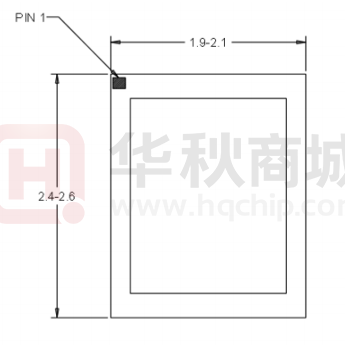
MDFN2.5×2-10 Package Outline Drawing
Bottom View
erg
yC
orp
.C
on
fi
de
nti
a
lP
Top View
Sil
Side View
Recommended PCB layout
(Reference Only)
Notes: 1, All dimension in millimeter and exclude mold flash & metal burr.
AN_SQ76003D Rev.0.9A
© 2021 Silergy Corp.
Silergy Corp. Confidential-prepared for Customer Use Only
14
All Rights Reserved.
�AN_SQ76003D
Taping & Reel Specification
rep
are
dF
or
K
IR
IT
RO
N
1. MDFN2.5×2 taping orientation
lP
Feeding direction
Package type
Sil
orp
erg
yC
Reel
Size
.C
on
fi
de
nti
a
2. Carrier Tape & Reel specification for packages
Tape width
(mm)
Pocket
pitch(mm)
Reel size
(Inch)
Trailer
length(mm)
Leader length
(mm)
Qty per
reel
8
4
7"
400
160
2500
MDFN2.5×2
3. Others: NA
AN_SQ76003D Rev.0.9A
© 2021 Silergy Corp.
Silergy Corp. Confidential-prepared for Customer Use Only
15
All Rights Reserved.
�AN_SQ76003D
Packaging Information\
Device Marking: a9
RO
N
Label Information
IR
IT
W/O: XXXXXXXXXX
P/N: SQ76003DAFM
rep
are
dF
QTY: 2500
D/C Lot: XXXXXXXXXX
Pb-Free
RoHS Compliant
Halogen Free
or
K
MSL1
Sil
erg
yC
orp
.C
on
fi
de
nti
a
lP
(The barcode is for demonstration only.)
AN_SQ76003D Rev.0.9A
© 2021 Silergy Corp.
Silergy Corp. Confidential-prepared for Customer Use Only
16
All Rights Reserved.
�AN_SQ76003D
IMPORTANT NOTICE
RO
N
1. Right to make changes. Silergy and its subsidiaries (hereafter Silergy) reserve the right to change any information
published in this document, including but not limited to circuitry, specification and/or product design, manufacturing or
descriptions, at any time and without notice. This document supersedes and replaces all information supplied prior to the
publication hereof. Buyers should obtain the latest relevant information before placing orders and should verify that such
information is current and complete. All semiconductor products are sold subject to Silergy’s standard terms and conditions of
sale.
rep
are
dF
or
K
IR
IT
2. Applications. Application examples that are described herein for any of these products are for illustrative purposes only.
Silergy makes no representation or warranty that such applications will be suitable for the specified use without further testing or
modification. Buyers are responsible for the design and operation of their applications and products using Silergy products.
Silergy or its subsidiaries assume no liability for any application assistance or designs of customer products. It is customer’s sole
responsibility to determine whether the Silergy product is suitable and fit for the customer’s applications and products planned.
To minimize the risks associated with customer’s products and applications, customer should provide adequate design and
operating safeguards. Customer represents and agrees that it has all the necessary expertise to create and implement safeguards
which anticipate dangerous consequences of failures, monitor failures and their consequences, lessen the likelihood of failures
that might cause harm and take appropriate remedial actions. Silergy assumes no liability related to any default, damage, costs or
problem in the customer’s applications or products, or the application or use by customer’s third-party buyers. Customer will
fully indemnify Silergy, its subsidiaries, and their representatives against any damages arising out of the use of any Silergy
components in safety-critical applications. It is also buyers’ sole responsibility to warrant and guarantee that any intellectual
property rights of a third party are not infringed upon when integrating Silergy products into any application. Silergy assumes no
responsibility for any said applications or for any use of any circuitry other than circuitry entirely embodied in a Silergy product.
de
nti
a
lP
3. Limited warranty and liability. Information furnished by Silergy in this document is believed to be accurate and reliable.
However, Silergy makes no representation or warranty, expressed or implied, as to the accuracy or completeness of such
information and shall have no liability for the consequences of use of such information. In no event shall Silergy be liable for
any indirect, incidental, punitive, special or consequential damages, including but not limited to lost profits, lost savings, business
interruption, costs related to the removal or replacement of any products or rework charges, whether or not such damages are
based on tort or negligence, warranty, breach of contract or any other legal theory. Notwithstanding any damages that customer
might incur for any reason whatsoever, Silergy’ aggregate and cumulative liability towards customer for the products described
herein shall be limited in accordance with the Standard Terms and Conditions of Sale of Silergy.
orp
.C
on
fi
4. Suitability for use. Customer acknowledges and agrees that it is solely responsible for compliance with all legal, regulatory
and safety-related requirements concerning its products, and any use of Silergy components in its applications, notwithstanding
any applications-related information or support that may be provided by Silergy. Silergy products are not designed, authorized or
warranted to be suitable for use in life support, life-critical or safety-critical systems or equipment, nor in applications where
failure or malfunction of an Silergy product can reasonably be expected to result in personal injury, death or severe property or
environmental damage. Silergy assumes no liability for inclusion and/or use of Silergy products in such equipment or
applications and therefore such inclusion and/or use is at the customer’s own risk.
erg
yC
5. Terms and conditions of commercial sale. Silergy products are sold subject to the standard terms and conditions of
commercial sale, as published at http://www.silergy.com/stdterms, unless otherwise agreed in a valid written individual
agreement specifically agreed to in writing by an authorized officer of Silergy. In case an individual agreement is concluded only
the terms and conditions of the respective agreement shall apply. Silergy hereby expressly objects to and denies the application
of any customer’s general terms and conditions with regard to the purchase of Silergy products by the customer.
Sil
6. No offer to sell or license. Nothing in this document may be interpreted or construed as an offer to sell products that is
open for acceptance or the grant, conveyance or implication of any license under any copyrights, patents or other industrial or
intellectual property rights. Silergy makes no representation or warranty that any license, either express or implied, is granted
under any patent right, copyright, mask work right, or other intellectual property right. Information published by Silergy
regarding third-party products or services does not constitute a license to use such products or services or a warranty or
endorsement thereof. Use of such information may require a license from a third party under the patents or other intellectual
property of the third party, or a license from Silergy under the patents or other intellectual property of Silergy.
For more information, please visit: www.silergy.com
© 2021 Silergy Corp.
AN_SQ76003D Rev.0.9A
© 2021 Silergy Corp.
Powered by TCPDF (www.tcpdf.org)
All Rights Reserved.
Silergy Corp. Confidential-prepared for Customer Use Only
17
All Rights Reserved.
�