Application Note: SY6818
High Current Overvoltage Protection Switch
With Integrated Reverse Blocking FET
Features
SY6818 is an over voltage protection switch with high
current capability to prevent damage to the downstream
system with low voltage rating. It achieves wide input
voltage range from 2.5VDC to 30VDC. Programmable OVP
is available with simple external resistor divider. Integrated
reverse blocking FET up to 20V rating prevents the leakage
current from output side to input side when the input power
supply is removed, but without output discharging.
Extremely low power path resistance RPWPT helps to reduce
power loss during the normal operation. Enable control is
available to cut off the energy path. High accuracy current
indicator is employed internally. It integrates the overtemperature protection shutdown and auto-recovery with
hysteresis to protect against over temperature events. It has
a default over current protection up to 5A internally and
auto-recovery. Each auto-recovery process is composed of
deglitch time TDG and switch turn-on time TON. This IC
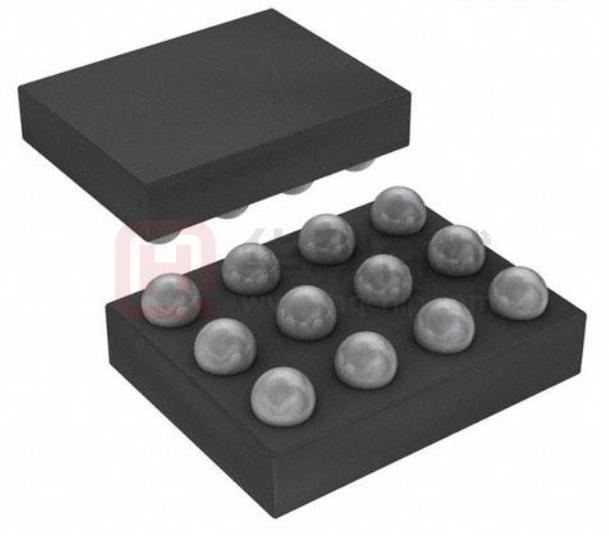
along with CSP-12, 1.73mmx1.73mm footprint provides
small PCB area application.
VIN=2.5V to 30V
Integrated reverse blocking FET up to 20V rating for
high voltage charging mode
Extremely Low Power Path Resistance RPWPT
RPWPT=53mΩ typ.
Programmable OVP thru external resistor divider,
accuracy up to +/-3%
Internal Soft Start to Prevent In-rush Current
Thermal Shutdown Protection & Auto Recovery
Current Indicator with High Accuracy up to +/-5%
RoHS Compliant and Halogen Free
Compact package: CSP-12 (1.73mmx1.73mm)
Ordering Information
SY6818 □(□□)□
Smart Phone
Tablet PCs
Mobile Device
on
fi
Temperature Code
Package Code
Optional Spec Code
Applications
de
nti
a
lP
rep
are
dF
or
W
OO
KO
O
General Description
Ordering Number
SY6818PLC
Package Type
Note
orp
.C
CSP1.73x1.73-12
yC
Typical Applications
CIN 1uF
Sil
erg
VIN
2.5-30V
ROVP1
COUT 1uF
IN
OUT
IN
IN
OUT
OUT
IN
SY6818
OVP
OUT
EN
ISNS
ROVP2
GND
VOUT
OFF
ON
RSNS
Figure 1. Schematic Diagram
AN_SY6818 Rev. 0.9B
© 2018 Silergy Corp.
Silergy Corp. Confidential-Prepared for Customer Use Only
1
All Rights Reserved.
�AN_SY6818
Pinout (top view)
A
B
C
ISNS
IN
OUT
GND
IN
OUT
OVP
IN
OUT
EN
IN
OUT
OO
KO
O
1
2
3
or
W
4
OUT
ISNS
C1,C2,C3,C4
A1
EN
A4
OVP
A3
GND
A2
Pin Description
Power input pin. Connect IN pin together. Decouple high frequency noise by connecting at
least 0.1uF MLCC to ground.
Output voltage pin. Connect OUT pins together for normal operation.
Current indicator pin. Connect a resister RSNS from this pin to ground. The current flow is
mirrored internally to charge RSNS for the indication. The ratio of power current to mirrored
current is 2.5k. The voltage on ISNS pin equals to VISNS=(IOUT/2.5k)*RSNS.
EN control pin. High logic enables all the internal circuit; low logic disables the internal
energy flow path.
External OVP program pin. Connect resistor divider to this pin to program the OVP
threshold. The internal reference is at 1.26V. Pull down this pin to ground to disable
external program function.
Power ground pin.
rep
are
Pin Number
B1,B2,B3,B4
de
nti
a
lP
Pin Name
IN
dF
①
Part Number
Package type
Top Mark
SY6818PLC
CSP1.73x1.73-12
ZQxyz
Note① : x=year code, y=week code, z= lot number code.
on
fi
Absolute Maximum Ratings (Note 1)
orp
.C
IN, EN, OVP, ---------------------------------------------------------------------------------------------------------------------------------------------------- 30V
OUT, -------------------------------------------------------------------------------------------------------------------------------------------------------------- 20V
ISNS, --------------------------------------------------------------------------------------------------------------------------------------------------------------- 6V
Continues IN, OUT current, ------------------------------------------------------------------------------------------------------------------------------------- 3A
Peak IN, OUT current (10ms), ---------------------------------------------------------------------------------------------------------------------------------- 5A
Power Dissipation, PD @ TA = 25°C CSP, -------------------------------------------------------------------------------------------------------------- 1.67 W
Package Thermal Resistance (Note 2)
yC
θ JA --------------------------------------------------------------------------------------------------------------------------------------------60 °C/W
θ JC --------------------------------------------------------------------------------------------------------------------------------------------- 7 °C/W
erg
Junction Temperature Range ------------------------------------------------------------------------------------------------------------------------------- 150°C
Lead Temperature (Soldering, 10 sec.) -------------------------------------------------------------------------------------------------------------------- 260°C
Storage Temperature Range ---------------------------------------------------------------------------------------------------------------------- -65°C to 150°C
Recommended Operating Conditions (Note 3)
Sil
IN, EN, OVP, ----------------------------------------------------------------------------------------------------------------------------------------- less than 30V
OUT, ---------------------------------------------------------------------------------------------------------------------------------------------------- less than 20V
ISNS, ---------------------------------------------------------------------------------------------------------------------------------------------------- less than 6V
Continues IN, OUT current, ------------------------------------------------------------------------------------------------------------------------- less than 3A
Peak IN, OUT current (10ms), ---------------------------------------------------------------------------------------------------------------------- less than 5A
Junction Temperature Range --------------------------------------------------------------------------------------------------------------------- -40°C to 125°C
Ambient Temperature Range ---------------------------------------------------------------------------------------------------------------------- -40°C to 85°C
AN_SY6818 Rev. 0.9B
© 2018 Silergy Corp.
Silergy Corp. Confidential-Prepared for Customer Use Only
2
All Rights Reserved.
�AN_SY6818
Block Diagram
OO
KO
O
Protection FET Reverse blocking FET
OUT
Soft
Start
Charge
Pump
Current
Sense
Control
Logic
EN
CTRL
ISNS
OVP
GND
rep
are
EN
dF
UVLO
or
W
IN
Sil
erg
yC
orp
.C
on
fi
de
nti
a
lP
Thermal
Detect
AN_SY6818 Rev. 0.9B
© 2018 Silergy Corp.
Silergy Corp. Confidential-Prepared for Customer Use Only
3
All Rights Reserved.
�AN_SY6818
Electrical Characteristics
(VIN = 2.5V to 30V, RISNS=1k, CIN=1uF, COUT=1uF, TA = 25°C, unless otherwise specified)
Symbol
VIN
VUVLO
VHYS
VRB
IBIAS
IRB
Shutdown Current
ISD
Enable Threshold
VEN
OVP Program Threshold
Resistance of Power Path
VOVP
RPWPT
Current Indicator Accuracy
VISNS
Maximum Current Capability Note4
Output Load Capacitance
IMAX
COUT
Deglitch Time
TDG
Switch Turn-On Time
TON
Thermal Shutdown Temperature
Thermal Shutdown Hysteresis
TSD
THYS
Test Conditions
Min
2.5
Typ
1.22
30
186
380
1.26
53
200
400
5
6
11
1000
16
Unit
V
V
V
V
µA
µA
µA
µA
V
V
V
mΩ
mV
mV
A
µF
ms
Max
30
2.4
0.7
1.2
1.7
ms
0.1
20
VIN=5V
VIN=0V, VOUT=16V, EN=0V
VIN=5V, EN=0V
VIN=30V, EN=0V
Rising
Falling
100
2
6
9
OO
KO
O
Parameter
Input Voltage Range
Input UVLO Threshold
UVLO Hysteresis
Reverse Blocking Range
Bias Current
Reverse Blocking Current
5
10
15
1.2
or
W
VIN=5V, IOUT=200mA, from IN to OUT
IOUT=0.5A, RSNS=1k
IOUT=1.0A, RSNS=1k
rep
are
dF
VIN=5V
Time from 2.5V
很抱歉,暂时无法提供与“SY6818PLC”相匹配的价格&库存,您可以联系我们找货
免费人工找货