SY7076
2V Minimum Input and 5. 5V Maximum Output
6A Peak Current Synchronous Boost with output current limit
General Description
Features
SY7076 is a high efficiency synchronous boost regulator
that converts down to 2V input and up to 5.5V output
voltage. It adopts NMOS for the main switch and PMOS
for the synchronous switch. It can disconnect the output
from input during the shutdown mode. It can program
output current limit by ILIM pin.
•
Ordering Information
•
•
•
•
•
SY7076 □(□□)□
•
Temperature Code
Package Code
Optional Spec Code
Package type
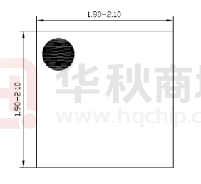
QFN2x2-10
•
•
•
Note
----
•
2V Minimum input voltage
Adjustable output voltage from 2.5V to 5.5V
6A peak current limit
Input under voltage lockout
Load disconnect during shutdown
Programmable output current limit protection
±10% output current limit accuracy
Force PWM mode selectable
Hic-cup mode for short protection
Low RDS(ON) (main switch/synchronous switch) at
5.0V output: 20/40mΩ
Output OVP protection
Compact package QFN2x2-10 package
Applications
导
小
芯
Ordering Number
SY7076QMC
•
All Single Cell Li or Dual Cell Battery Operated
Products as MP-3 Player, PDAs, and Other
Portable Equipment.
l-F
or
半
•
Typical Applications
en
tia
Efficiency, PFM mode
100
MODE
SOUT
IN
98
VOUT=5V
on
Li-on Battery Input
L
1.5uH
yC
CIN
22uF×2
Sil
erg
0Ω
LX
POUT
RH
470k
ILIM
FB
CILIM
10nF
RILIM
50kΩ
RL
148.4k
EN PGND SGND
COUT
22uF×3
Efficiency (%)
1uF
fid
1uF
96
94
92
90
VIN=2.5V, VOUT=5V
VIN=3.3V, VOUT=5V
VIN=4.2V, VOUT=5V
88
86
Note: The minimum recommended value for CILIM is 10nF.
0.001
0.01
0.1
1
10
Load Current (A)
Figure 1. Schematic Diagram
SY7076 Rev. 0.9
© 2018 Silergy Corp.
Figure 2. Efficiency vs. Load Current
Silergy Corp. Confidential- Prepared for Customer Use Only
All Rights Reserved.
1
�SY7076
Pinout (top view)
10
9
FB
ILIM
1
8
MODE
POUT
2
LX
3
PGND
7
EN
SOUT
6
IN
5
SGND
4
(QFN2x2-10)
Top mark: Fnxyz (Device code: Fn, x=year code, y=week code, z= lot number code)
Description
MODE
8
ILIM
9
FB
10
芯
7
导
小
EN
半
6
l-F
or
SOUT
Power output pin. Decouple this pin to GND pin with at least 2pcs 22uF ceramic cap.
Inductor node. Connect an inductor between IN pin and LX pin.
Power ground pin.
Signal ground pin.
Signal input pin. Decouple this pin to GND with at least 4.7uF ceramic cap.
Signal output pin. Decouple this pin to GND pin with at least 1uF ceramic cap for noise
immunity consideration.
Enable pin. Internal integrated with 1MΩ pull down resistor.
PFM/PWM select pin. Low for auto PFM/PWM mode. High for force PWM mode.
Internal integrated with 1MΩ pull down resistor.
Current limit program pin, program output current limit by connecting resister and
capacitor parallel network to ground.
ILIM(A)=100k/RILIM(Ω). CILIM must be large than 10nF.
Feedback pin. Connect a resistor R1 between OUT and FB, and a resistor R2 between
FB and GND to program the output voltage. VOUT=1.2V× (RH/RL+1).
tia
1
2
3
4
5
Sil
erg
yC
on
fid
en
Name
POUT
LX
PGND
SGND
IN
SY7076 Rev. 0.9
© 2018 Silergy Corp.
Silergy Corp. Confidential- Prepared for Customer Use Only
All Rights Reserved.
2
�SY7076
Block Diagram
MODE
SOUT
VCC
IN
Output
current
sense
IN
SOUT
IN
ILIM
GM
POUT
VCC
Supply
ZC2
1.2V
Ref
TG
FB
GM
WELL
SWITCH
PWM
Control
LX
BG
ZC1
1.2V
Ref
SGND
Current
Sense
PGND
Enable
control
芯
EN
半
导
小
Figure 3. Block Diagram
l-F
or
Absolute Maximum Ratings (Note 1)
yC
on
fid
en
tia
LX--------------------------------------------------------------------------------------------------------------- -----------------8.0V
All other Pins-------------------------------------------------------------------------------------------------------------------6.0V
Power Dissipation, PD@ TA=25°C, QFN2x2-10--------------------------------------------------------------------------2.5W
Package Thermal Resistance (Note 2)
θ JA ----------------------------------------------------------------------------------------------- ----------------50°C/W
θ JC ---------------------------------------------------------------------------------------------------------------10°C/W
Junction Temperature Range --------------------------------------------------------------------------------------------- 150°C
Lead Temperature (Soldering, 10 sec.) --------------------------------------------------------------------------------- 260°C
Storage Temperature Range ----------------------------------------------------------------------------------- -65°C to 150°C
Sil
erg
Recommended Operating Conditions (Note 3)
IN --------------------------------------------------------------------------------------------------------------------- 2.0V to 5.5V
OUT------------------------------------------------------------------------------------------------------------------- 2.5V to 5.5V
All other pins --------------------------------------------------------------------------------------------------------------- 0-5.5V
Junction Temperature Range ---------------------------------------------------------------------------------- -40°C to 125°C
Ambient Temperature Range ----------------------------------------------------------------------------------- -40°C to 85°C
SY7076 Rev. 0.9
© 2018 Silergy Corp.
Silergy Corp. Confidential- Prepared for Customer Use Only
All Rights Reserved.
3
�SY7076
Electrical Characteristics
(VIN =3.0V, VOUT=4.2V, IOUT=500mA, TA = 25°C unless otherwise specified)
Symbol
VIN
VOUT
IQ
Min
2
2.5
Io=0A,VEN=VIN=3.0V,
VOUT=5.0V
VEN=0V, VIN=3.0V
VOUT
很抱歉,暂时无法提供与“SY7076QMC”相匹配的价格&库存,您可以联系我们找货
免费人工找货