Application Note: SY98110
4.5-16V Input, 15A Output, Step Down DC/DC Converter
Features
The SY98110 adopts the instant PWM architecture to
achieve fast transient responses for high step down
applications. The device is also equipped with cycle-bycycle current limit, hiccup over current protection and
thermal shutdown protection.
yC
erg
Sil
VOUT
VIN
+
Ce
Telecom and Networking Systems
Servers
High power access points
Storage systems
Cellular base stations
.C
orp
VIN:4.5-16V
Note
--
on
fi
Package Type
QFN7×8-52
Applications
de
nti
a
Temperature Code
Package Code
Optional Spec Code
lP
SY98110 □(□□)□
Typical Applications
RO
N
rep
are
Ordering Information
Ordering Number
SY98110VVC
IR
IT
Wide Input Voltage Range: 4.5V to 16V.
Capable of 15A Constant Output Current
High Output Voltage Accuracy Over Temperature
Range
Instant PWM Architecture to Achieve Fast
Transient Response
Pseudo 600kHz, 800kHz and 1000kHz Switching
Frequency Selection
Reliable Protection Mode:
Auto-recovery Mode for UVP, UVLO,
OTP and OVP
Hic-cup Mode for OCP and SCP
Start-up with Pre-biased Voltage
Adjustable Input Voltage UVLO by EN Pin
Adjustable Soft-start Time Limits the Inrush
Current
Remote Sensing at Point of Load Side
Power Good Indicator
Compact Package: QFN7×8-52
or
K
The SY98110 operates over a wide input voltage range
from 4.5V to 16V which is suitable for 12V input voltage
application. And it is capable of delivering 15A output
current over a wide ambient temperature range. The
efficiency is pretty high because it integrates high quality
main switch, synchronous switch and inductor inside to
minimize the conduction loss. It provides accurate
regulation for a variety of loads over all operation
temperature range.
dF
General Description
VOUT
CIN
Cff
RH
To EN Control
EN
FB
SS
SENSEPG
COUT
Load
RL
CSS
RPG
MODE
VCC
RMODE
CVCC
GND
AGND
RGND
Figure 1. Schematic Diagram
AN_SY98110 Rev.0.9
© 2020 Silergy Corp.
Silergy Corp. Confidential-Prepared for Customer Use Only
1
All Rights Reserved.
�SY98110
27 AGND
28 PG
30 EN
29 AGND
31 FB
32 SENSE-
33 SS
35 NC
34 MODE
37 AGND
36 AGND
39 VOUT
38 VOUT
Pinout (top view)
VOUT
39
VOUT
40
VOUT
41
VOUT
VOUT
42
43
24 VIN
23 VIN
VOUT
44
22 VIN
VOUT
45
21 VIN
27 AGND
IR
IT
25 AGND
RO
N
26 AGND
EP1
AGND
20 VIN
GND 46
GND 47
19 VIN
GND 48
or
K
EP2
GND
18 VIN
17 GND
GND 49
16 GND
GND 50
GND 51
dF
15 GND
14 GND
GND 1
13
GND
12 GND
13 GND
11 GND
10 GND
9 GND
8 GND
7 GND
6 GND
5 GND
4 VCC
3 NC
2 AGND
1 GND
rep
are
GND 52
33
MODE
34
VOUT
38-45
AN_SY98110 Rev.0.9
© 2020 Silergy Corp.
Silergy Corp. Confidential-Prepared for Customer Use Only
2
All Rights Reserved.
3, 35
VCC
4
VIN
18-24
PG
28
EN
30
SENSE-
yC
erg
31
Sil
FB
.C
NC
on
fi
SS
Pin Description
Ground pins.
Analog ground pins. Only connect pin2 to GND. Refer to layout suggestion for
details.
Do not connect these pins to AGND, to another pin, or to any other voltage. These
pins are connected to internal circuitry. Each pin must be soldered to an isolated
pad.
Internal 3.3V LDO output. Power supply for internal analog circuits and driving
circuit. Decouple this pin to GND with at least a 1μF ceramic capacitor.
Input pin. Decouple this pin to the GND pin with at least a 30μF ceramic capacitor.
Power good Indicator. Open drain output when the output voltage is within 90% to
120% of regulation point.
Enable control. Pull this pin high to turn on the IC. Can be used for setting the on
and off threshold (adjust UVLO) with two additional resistors. Do not leave this
pin floating.
Output feedback pin. Connect this pin (as shown in Figure 1) to program the output
voltage.
Negative output voltage sensing pin. It can be connected to the load negative
terminal to compensate power line voltage drop. If this function is not needed,
connect this pin to the closest GND pin.
Soft-start programming pin. Connect a capacitor from this pin to ground to
program the soft-start time. Leave this pin open for default 1.3ms soft-start.
Operation mode selection pin. Program this pin the select FCCM or PFM mode,
and the switching frequency.
Output pin. Decouple this pin to GND pin with at least 6×22μF ceramic capacitors.
AGND
Pin Number
1, 5-17, 46-52
2, 25-27, 29,
36-37
orp
Pin Name
GND
de
nti
a
lP
(QFN7×8-52)
Top Mark: DCRxyz (device code: DCR, x=year code, y=week code, z= lot number code)
32
�SY98110
IN
VCC
Input
UVLO
VCC
UVLO
3.3V LDO
Current
Sense
VCC
RO
N
Bcotstrap
Charge
EN
MODE
CBS
OVP
Current
Sense
VCC
dF
UVP
FB
rep
are
DIFF
SENSE-
GND
Discharge
SoftStart
AGND
lP
SS
Vout
L
or
K
PWM
Control &
Protection
Logic
OTP
IR
IT
PG
de
nti
a
Figure2. Block Diagram
Absolute Maximum Ratings (Note 1)
on
fi
Supply Input Voltage------------------------------------------------------------------------------------------------- -0.3V to 18V
FB, SENSE-, AGND, VCC, PG Voltage-------------------------------------------------------------------------- -0.3V to 4V
All Other Pins ------------------------------------------------------------------------------------------------- -0.3V to VIN+0.3V
Power Dissipation, PD @ TA = 25°C --------------------------------------------------------------------------------------- 7.6W
Package Thermal Resistance (Note 2)
.C
θ JA ------------------------------------------------------------- -------------------------------------------------13.1°C/W
yC
orp
Lead Temperature (Soldering, 10 sec.) ------------------------------------------------------------------------------------ 260°C
Storage Temperature Range -------------------------------------------------------------------------------------- -65°C to 150°C
Operation Internal Temperature Range ------------------------------------------------------------------------- -40°C to 150°C
Recommended Operating Conditions (Note 3)
Sil
erg
Supply Input Voltage -------------------------------------------------------------------------------------------------- 4.5V to 16V
Output Voltage --------------------------------------------------------------------------------------------------- 0.6V to 6.5V
Output Current Range--------------------------------------------------------------------------------------------0A to 15A
Operating Junction Temp.(T J) ----------------------------------------------------------------------------- -40℃ to +125℃
AN_SY98110 Rev.0.9
© 2020 Silergy Corp.
Silergy Corp. Confidential-Prepared for Customer Use Only
3
All Rights Reserved.
�SY98110
Electrical Characteristics
Sil
erg
yC
orp
.C
on
fi
de
nti
a
lP
rep
are
dF
or
K
IR
IT
RO
N
(VIN = 12V, VOUT =3.3V, IOUT = 15A, COUT = 6×22µF, RMODE=30kΩ, TA = 25°C, FB divider resistor accuracy =
0.5%, unless otherwise specified)
Parameter
Symbol Test Conditions
Min
Typ
Max
Unit
Input Specifications
Input Voltage Range
VIN
4.5
16
V
Input UVLO Threshold (rising) VUVLO
EN=VIN
4.2
V
Input UVLO Threshold
VHYS
200
mV
Hysteresis
IIN, NULL
Input Current with No Load
VIN=12V, IO=0A
36
60
80
mA
IIN, FULL
Input Current with Full Load
VIN=12V, IO=15A
4.4
4.6
5.5
A
ISD
Shutdown Current
VIN=12V, EN=0
2.5
μA
Output Specifications
∆VLNR
Line Regulation
VIN=5-16V, TA=25°C, IO=15A
-1.5
1
%
VIN=12V, TA=-40°C to 85°C,
Temperature Regulation
∆T
-1
2
%
IO=7.5A
ILIMT
Output Current Limit
Protection Mode: Hiccup
16
20
24
A
From 10% to 90% of output setRise Time
tRISE
Point, CSS open, start up from
0.6
1
1.4
ms
EN
VOVP
VOUT OVP
110
120
130 %Vo,setpoint
VUVP
VOUT UVP
45
50
55
%Vo,setpoint
tUVP,DLY
VOUT UVP Delay Time
20
µs
General Specifications
RMODE=0Ω,IOUT=0A,FCCM,
480
600
720
kHz
VOUT=1V, TJ=25°C
RMODE=30.1kΩ,IOUT=0A,FCCM,
Switching Frequency
fSW
640
800
960
kHz
VOUT=1V, TJ=25°C
RMODE=60.4kΩ,IOUT=0A,FCCM,
800
1000 1200
kHz
VOUT=1V, TJ=25°C
Thermal Shutdown
TSD
OTP Mode: auto recovery
160
°C
Temperature
Thermal Shutdown Hysteresis THYS
30
°C
Min ON Time (Note 4)
tON,MIN
IOUT=3A
60
ns
Min OFF Time (Note 4)
tOFF,MIN
IOUT=3A
180
ns
Control and Indicator Signals
EN Input Voltage High
VEN,H
VIN=12V, IO=0A
1.1
1.2
1.5
V
EN Input Voltage Low
VEN,L
VIN=12V, IO=0A
0.9
1
1.3
V
VEN,HYS
EN Hysteresis
0.2
V
VFB falling, PG high to low
77
80
84
%VREF
VFB rising, PG low to high
89.5
92.5
96.5 %VREF
Power Good Threshold
VPG
VFB rising, PG high to low
110
120
130 %VREF
VFB falling, PG low to high
102
105
108 %VREF
Power Good Asserts Delay
tPG
0.8
ms
(Note 4)
Power Good Sink Current
IPG,SINK
VPG=0.4V
10
mA
Capability
IPG, LKG
Power Good Leakage Current
VPG=3.3V
3
5
μA
VCC
VCC Voltage
IVCC=0mA
3.18
3.3
3.42
V
VREF
-40°C 0.4V), or
thermal shutdown, so that the output voltage can be
discharged in a minimal time, even when the load
current is zero. The discharge FET in parallel with
the low-side synchronous rectifier turns on after the
low-side synchronous rectifier turns off when shut
down logic is triggered.
When operating in FCCM light load mode, if the
output voltage remains higher than the OVP level, the
lower-side MOSFETS keeps on until the reverse
current limit (~-13A) is triggered to discharge the
output voltage.
lP
It is not recommended to connect EN and VIN
directly. A 10kΩ resistor should be used if EN is
pulled high by VIN.
RO
N
Enable Control
The EN input is a high-voltage capable input with
logic-compatible threshold. The comparator design
scheme makes the EN rising threshold accurate
comparatively. When EN voltage rises to ~0.8V,
VCC works so that the EN comparator has source
supply. When EN is driven above 1.23V normal
device operation will be enabled, and the switching
node pulse appear. When EN voltage falls lower than
EN rising threshold for one hysteresis, the switching
node pulse is inhibited. When EN voltage is driven <
0.4V the VCC will be shut down, reducing input
current to < 5μA (Normal temperature).
Over Temperature Protection (OTP)
The module includes OTP circuitry to prevent
overheating due to excessive power dissipation. This
will shut down the device when the die temperature
exceeds 160°C. Once the die temperature cools down
by approximately 30°C, the device will resume
normal operation. For continuous operation, provide
adequate cooling so that the die temperature does not
exceed the OTP threshold.
Pre-bias Startup
If the output is pre-biased to a certain voltage before
start-up, the device disables the switching of both the
high-side power switch and the low-side synchronous
rectifier until the voltage on the internal soft start
SS pin voltage exceeds the sensed output voltage at
the FB node. Before the switching node pulse occurs,
the switching node voltage is sampled to internal ontime generator circuit to generate the first on-time, so
that the first on-time will match the current pre-bias
output voltage.
Silergy Corp. Confidential-Prepared for Customer Use Only
11
All Rights Reserved.
�SY98110
Capacitance
6×22μF
Vendor
murata
2) CIN must be close to the VIN and GND pins. The
loop area formed by CIN and GND must be
minimized.
IR
IT
COUT
Layout Design
For the minimum noise consideration, following
components should be close to the IC: CIN and COUT.
1) It is desirable to maximize the PCB copper area
connecting to the GND pin to achieve the best
thermal and noise performance. If the board
space allowed, a ground plane is highly desirable.
RO
N
Output Capacitor COUT
The output capacitor is selected to reduce the output
ripple noise. Both steady state ripple and transient
requirements must be taken into consideration when
selecting this capacitor. For the best performance, it
is recommended to use an X7R or better grade
ceramic capacitor with 16V rating and greater than
132μF capacitance. Place this ceramic capacitor
really close to the OUT and GND pins to minimize
the loop area formed by COUT, and the OUT/GND
pins.
3) It’s recommended to connect AGND and GND
at a single point, close to the corresponding
capacitors. Please refer to the detail in the
following layout demonstration.
PN
GRM31CC71C226ME11L
dF
or
K
If the output capacitance is larger than 800μF
(ceramic) or other type of capacitor (polymer ,
tantalum…) is used, please contact Silergy
supporting team to get more assessment.
VIN
+
CIN3
CIN2
CIN4
R3
To EN Control
EN
FB
SS
SENSEPG
C3
COUT1
COUT2
COUT3
COUT4 COUT5 COUT6
Load
lP
CIN1
VOUT
rep
are
VOUT
VIN:4.5-16V
C2
de
nti
a
R4
R1
MODE
R2
C1
AGND
on
fi
GND
VCC
Sil
erg
yC
orp
.C
R5
Figure3. PCB Layout Suggestion
AN_SY98110 Rev.0.9
© 2020 Silergy Corp.
Silergy Corp. Confidential-Prepared for Customer Use Only
12
All Rights Reserved.
�SY98110
R4
RO
N
Murata
Murata
Murata
Murata
Murata
Murata
Murata
Murata
Murata
Murata
GRM1885C1H472JA01D
Murata
fsw:600kHz
VOUT=0.6V
VOUT=1.2V
VOUT=1.8V
VOUT=3.3V
VOUT=5V
Sil
erg
yC
orp
.C
on
fi
de
nti
a
lP
R5
GGM31CC71E106KA03#
GGM31CC71E106KA03#
GGM31CC71E106KA03#
GRM31CC71C226ME11L
GRM31CC71C226ME11L
GRM31CC71C226ME11L
GRM31CC71C226ME11L
GRM31CC71C226ME11L
GRM31CC71C226ME11L
GGM188R71C105MA64#
Note
IR
IT
CIN2
CIN3
CIN4
COUT1
COUT2
COUT3
COUT4
COUT5
COUT6
C1
C2
C3
R1
R2
R3
Manufacturer
or
K
CIN1
Part Number
dF
Description
100µF/25V
Electrolytic Capacitor
10µF,25V,X7R,1206
10µF,25V,X7R,1206
10µF,25V,X7R,1206
22µF, 16V, X7S, 1206
22µF, 16V, X7S, 1206
22µF, 16V, X7S, 1206
22µF, 16V, X7S, 1206
22µF, 16V, X7S, 1206
22µF, 16V, X7S, 1206
1µF, 6.3V, 0603
NA
4.7nF, 50V, C0G, 0603
100kΩ, 0603
0Ω, 0603
2kΩ, 0603
5MΩ, 0603
2kΩ, 0603
1kΩ, 0603
0.442kΩ, 0603
0.274kΩ, 0603
0Ω, 0603
rep
are
Reference Designator
AN_SY98110 Rev.0.9
© 2020 Silergy Corp.
Silergy Corp. Confidential-Prepared for Customer Use Only
13
All Rights Reserved.
�SY98110
rep
are
dF
or
K
IR
IT
RO
N
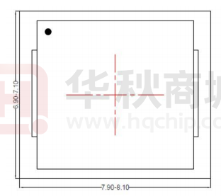
QFN7×8-52 Package Outline Drawing
Bottom View
erg
yC
orp
.C
on
fi
de
nti
a
lP
Top View
Sil
Front View
Recommended PCB layout
(Reference only)
Notes: 1, All dimension in millimeter and exclude mold flash & metal burr;
2, center line refers chip body center
AN_SY98110 Rev.0.9
© 2020 Silergy Corp.
Silergy Corp. Confidential-Prepared for Customer Use Only
14
All Rights Reserved.
�SY98110
Taping & Reel Specification
1. Taping Orientation
Feeding Direction
rep
are
dF
or
K
IR
IT
RO
N
QFN8.0×7.0
on
fi
de
nti
a
lP
2. Carrier Tape & Reel specification for packages
Sil
erg
yC
orp
.C
Reel
Size
Package types
Tape
width
(mm)
Pocket
pitch(mm)
QFN8.0×7.0
16
12
AN_SY98110 Rev.0.9
© 2020 Silergy Corp.
Reel size
Trailer *
(Inch)
length(mm)
13"
600
Leader *
length (mm)
Qty per
reel
(pcs)
600
800
Silergy Corp. Confidential-Prepared for Customer Use Only
15
All Rights Reserved.
�SY98110
IMPORTANT NOTICE
RO
N
1. Right to make changes. Silergy and its subsidiaries (hereafter Silergy) reserve the right to change any information
published in this document, including but not limited to circuitry, specification and/or product design, manufacturing or
descriptions, at any time and without notice. This document supersedes and replaces all information supplied prior to the
publication hereof. Buyers should obtain the latest relevant information before placing orders and should verify that such
information is current and complete. All semiconductor products are sold subject to Silergy’s standard terms and conditions of
sale.
rep
are
dF
or
K
IR
IT
2. Applications. Application examples that are described herein for any of these products are for illustrative purposes only.
Silergy makes no representation or warranty that such applications will be suitable for the specified use without further testing or
modification. Buyers are responsible for the design and operation of their applications and products using Silergy products.
Silergy or its subsidiaries assume no liability for any application assistance or designs of customer products. It is customer’s sole
responsibility to determine whether the Silergy product is suitable and fit for the customer’s applications and products planned.
To minimize the risks associated with customer’s products and applications, customer should provide adequate design and
operating safeguards. Customer represents and agrees that it has all the necessary expertise to create and implement safeguards
which anticipate dangerous consequences of failures, monitor failures and their consequences, lessen the likelihood of failures
that might cause harm and take appropriate remedial actions. Silergy assumes no liability related to any default, damage, costs or
problem in the customer’s applications or products, or the application or use by customer’s third-party buyers. Customer will
fully indemnify Silergy, its subsidiaries, and their representatives against any damages arising out of the use of any Silergy
components in safety-critical applications. It is also buyers’ sole responsibility to warrant and guarantee that any intellectual
property rights of a third party are not infringed upon when integrating Silergy products into any application. Silergy assumes no
responsibility for any said applications or for any use of any circuitry other than circuitry entirely embodied in a Silergy product.
de
nti
a
lP
3. Limited warranty and liability. Information furnished by Silergy in this document is believed to be accurate and reliable.
However, Silergy makes no representation or warranty, expressed or implied, as to the accuracy or completeness of such
information and shall have no liability for the consequences of use of such information. In no event shall Silergy be liable for
any indirect, incidental, punitive, special or consequential damages, including but not limited to lost profits, lost savings, business
interruption, costs related to the removal or replacement of any products or rework charges, whether or not such damages are
based on tort or negligence, warranty, breach of contract or any other legal theory. Notwithstanding any damages that customer
might incur for any reason whatsoever, Silergy’ aggregate and cumulative liability towards customer for the products described
herein shall be limited in accordance with the Standard Terms and Conditions of Sale of Silergy.
orp
.C
on
fi
4. Suitability for use. Customer acknowledges and agrees that it is solely responsible for compliance with all legal, regulatory
and safety-related requirements concerning its products, and any use of Silergy components in its applications, notwithstanding
any applications-related information or support that may be provided by Silergy. Silergy products are not designed, authorized or
warranted to be suitable for use in life support, life-critical or safety-critical systems or equipment, nor in applications where
failure or malfunction of an Silergy product can reasonably be expected to result in personal injury, death or severe property or
environmental damage. Silergy assumes no liability for inclusion and/or use of Silergy products in such equipment or
applications and therefore such inclusion and/or use is at the customer’s own risk.
erg
yC
5. Terms and conditions of commercial sale. Silergy products are sold subject to the standard terms and conditions of
commercial sale, as published at http://www.silergy.com/stdterms, unless otherwise agreed in a valid written individual
agreement specifically agreed to in writing by an authorized officer of Silergy. In case an individual agreement is concluded only
the terms and conditions of the respective agreement shall apply. Silergy hereby expressly objects to and denies the application
of any customer’s general terms and conditions with regard to the purchase of Silergy products by the customer.
Sil
6. No offer to sell or license. Nothing in this document may be interpreted or construed as an offer to sell products that is
open for acceptance or the grant, conveyance or implication of any license under any copyrights, patents or other industrial or
intellectual property rights. Silergy makes no representation or warranty that any license, either express or implied, is granted
under any patent right, copyright, mask work right, or other intellectual property right. Information published by Silergy
regarding third-party products or services does not constitute a license to use such products or services or a warranty or
endorsement thereof. Use of such information may require a license from a third party under the patents or other intellectual
property of the third party, or a license from Silergy under the patents or other intellectual property of Silergy.
For more information, please visit: www.silergy.com
© 2020 Silergy Corp.
AN_SY98110 Rev.0.9
© 2020 Silergy Corp.
Powered by TCPDF (www.tcpdf.org)
All Rights Reserved.
Silergy Corp. Confidential-Prepared for Customer Use Only
16
All Rights Reserved.
�