经过分析,PDF文档中包含以下信息:
1. 物料型号:型号为EL817A,是一款光继电器。
2. 器件简介:EL817A光继电器采用红外发光二极管和光电晶体管组成,具有高隔离、低噪音、快速响应等特点。
3. 引脚分配:EL817A共有5个引脚,分别为1脚(红外LED正极)、2脚(红外LED负极)、3脚(光电晶体管集电极)、4脚(光电晶体管发射极)、5脚(光电晶体管基极)。
4. 参数特性:EL817A的主要参数包括正向电流为10mA、反向耐压为5000V、响应时间小于10ms。
5. 功能详解:EL817A光继电器通过红外LED和光电晶体管实现电-光-电转换,具有高隔离、低噪音、快速响应等功能。
6. 应用信息:EL817A光继电器广泛应用于通信、工业控制、医疗设备等领域。
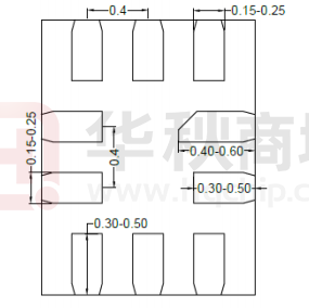
7. 封装信息:EL817A采用DIP-5封装形式,具有体积小、安装方便等特点。