Application Note: SQ52201
36V High-accuracy Current/Power Monitor
With Programmable Alert Function
General Description
Features
The SQ52201 is a high accuracy current shunt, bus
voltage and power monitor with an I2C or SMBUScompatible interface.
The shunt voltage drop and the bus supply voltage
are both sampled accurately in the device. The
sampled data are processed inside the device to
generate the power data with programmable
calibration, averaging technique and internal
multiplier. Programmable alert function provides
abundant alert sources settings and makes the
application system more reliable.
The SQ52201 senses current on common mode bus
voltages that can vary from 0V to 36V, independent
of the supply voltage. The device operates from a
single 2.7V to 5.5V supply. The SQ52201 is
specified over the operating temperature range
between –40°C and +125°C and features up to 16
programmable addresses on the I2C-compatible
interface.
Applications
The SQ52201 is available in the MSOP-10 package.
Ordering Information
SQ52201 □(□□)□
Temperature Code
Package Code
Optional Spec Code
Ordering Number
SQ52201FBC
Package type
MSOP10
Senses Bus Voltages from 0 V to 36 V
High-Side or Low-Side Sensing
Bi-directional Current Sensing
Reports Current, Voltage, and Power
High Accuracy:
0.02% Gain Error (Typ) for Shunt Voltage
0.02% Gain Error (Typ) for Bus Voltage
2.5μV Offset (Typ) for Shunt Voltage
1.25mV Offset (Typ) for Bus Voltage
Configurable Averaging Options
Configurable Conversion Time
Abundant Alert Sources Setting
16 Programmable Addresses
High Speed I2C Mode Compatible
Operates from 2.7V to 5.5V Power Supply
Servers
Telecom Equipment
Computing
Power Management
Battery Chargers
Power Supplies
Test Equipment
Note
--
Typical Application
2.7 ~ 5.5V
Power Supply
0 ~ 36V
VBUS
VS
High-side
shunt
SDA
LOAD
IN+
SCL
IN-
MCU
Alert
A0
GND
A1
Figure 1. Typical Application
AN_SQ52201 Rev. 0.9
© 2021 Silergy Corp.
Silergy Corp. Confidential- Prepared for Customer Use Only
1
All Rights Reserved.
�AN_SQ52201
Pin out
(Top View)
Top Mark:
A1
1
10
IN+
A0
2
9
IN-
Alert
3
8
VBUS
SDA
4
7
GND
SCL
5
6
VS
(MSOP10)
CXExyz, (Device code: CXE, x=year code, y=week code, z= lot number code)
Pin No.
1
2
3
4
5
6
7
8
Pin Name
A1
A0
Alert
SDA
SCL
VS
GND
VBUS
9
IN–
10
IN+
Pin Description
Address pin. Connect to GND, SCL, SDA, or VS.
Address pin. Connect to GND, SCL, SDA, or VS.
Multi-functional alert, open-drain output.
Serial bus data line, open-drain input/output.
Serial bus clock line, open-drain input.
Power supply, 2.7 V to 5.5 V.
Ground.
Bus voltage input.
Negative differential voltage input. Connect to load side of shunt
resistor.
Positive differential voltage input. Connect to supply side of shunt
resistor.
Block Diagram
2.7 ~ 5.5V
Power Supply
0 ~ 36V
VS
VBUS
High-side
shunt
V
Current Register
LOAD
SDA
Power Register
IN+
ADC
Voltage Register
INLow-side
shunt
I
SCL
I2C or
SMBus
Compatible
Interface
Alert
A0
A1
Alert Register
GND
Figure 2. Block Diagram
AN_SQ52201 Rev. 0.9
© 2021 Silergy Corp.
Silergy Corp. Confidential- Prepared for Customer Use Only
2
All Rights Reserved.
�AN_SQ52201
Absolute Maximum Ratings (Note 1)
VS ----------------------------------------------------------------------------------------------------------------------- -0.3V to 6V
Differential Analog input (VIN+ – VIN-) -------------------------------------------------------------------------- -40V to +40V
Common Mode Analog input (VIN+ + VIN-) / 2 ------------------------------------------------------------------ -0.3V to 40V
VBUS------------------------------------------------------------------------------------------------------------------ -0.3V to 40V
VSDA --------------------------------------------------------------------------------------------------------------------- -0.3V to 6V
VSCL ------------------------------------------------------------------------------------------------------------- -0.3V to VS+0.3V
Input current into any pin ------------------------------------------------------------------------------------------------------ 5mA
Open-drain digital output current-------------------------------------------------------------------------------------------- 10mA
Power Dissipation, PD @ TA = 25°C--------------------------------------------------------------------------------------- 0.74W
Package Thermal Resistance (Note 2)
θ JA ------------------------------------------------------------------------------------------------------------- 136°C/W
θ JC --------------------------------------------------------------------------------------------------------------- 25°C/W
Junction Temperature Range------------------------------------------------------------------------------------------------- 150°C
Storage Temperature Range ------------------------------------------------------------------------------------- -65°C to 150°C
ESD Susceptibility
HBM (Human Body Mode) ---------------------------------------------------------------------------------------------------- 2kV
CDM ------------------------------------------------------------------------------------------------------------------------------- 1kV
Recommended Operating Conditions
VS --------------------------------------------------------------------------------------------------------------------------------- 3.3V
Common Mode Analog input (VIN+ + VIN-) / 2 ------------------------------------------------------------------------------ 12V
Operation Temperature Range----------------------------------------------------------------------------------- -40°C to 125°C
AN_SQ52201 Rev. 0.9
© 2021 Silergy Corp.
Silergy Corp. Confidential- Prepared for Customer Use Only
3
All Rights Reserved.
�AN_SQ52201
Electrical Characteristics
VS = 3.3V, VIN+ = 12V, VSENSE = (VIN+ – VIN–) = 0mV and VVBUS = 12V, TA = 25°C unless otherwise specified
Parameter
Input
Symbol
Conditions
Shunt Voltage Input Range
Bus Voltage Input Range
(Note 3)
Common-Mode Rejection
Shunt Offset Voltage, RTI
(Note 4)
Shunt Offset Voltage, RTI vs.
Temperature (Note 4)
Shunt Offset Voltage, RTI vs.
Power Supply (Note 4)
Bus Offset Voltage, RTI
(Note 4)
Bus Offset Voltage, RTI vs.
Temperature (Note 4)
Bus Offset Voltage, RTI vs.
Power Supply (Note 4)
Input Bias Current (IIN+, IIN)
VBUS Input Impedance
CMRR
0V≤VIN+≤36V
+81.91
75
mV
0
36
V
140
dB
–40°C≤TA≤125°C
0.02
0.1
μV/°C
2.7V≤VS≤5.5V
2.5
–40°C≤TA≤125°C
μV/V
±1.25
±7.5
mV
10
40
μV/°C
PSRR
0.5
mV/V
IB
7
830
μA
kΩ
1 LSB Step Size
Shunt Voltage Gain Error
Shunt Voltage Gain Error vs.
Temperature
Bus Voltage Gain Error
Bus Voltage Gain Error vs.
Temperature
Differential Nonlinearity
(IN+ pin) + (IN– pin),
Power-down mode
0.1
Shunt voltage
Bus voltage
–40°C≤TA≤125°C
–40°C≤TA≤125°C
tCT
CT bit = 000
CT bit = 001
CT bit = 010
CT bit = 011
CT bit = 100
CT bit = 101
CT bit = 110
CT bit = 111
SMBus
Smbus Timeout (Note 6)
Digital Input/Output
Input Capacitance
AN_SQ52201 Rev. 0.9
© 2021 Silergy Corp.
-81.92
μV
DC Accuracy
ADC Native Resolution
Leakage Input Current
Units
±10
VOS
Input Leakage (Note 5)
ADC Conversion Time
Max
126
Typ
±2.5
VOS
PSRR
Min
0.5
μA
16
2.5
1.25
0.02
0.15
Bits
μV
mV
%
10
50
ppm/°C
0.02
0.2
%
10
50
ppm/°C
±0.1
140
204
332
588
1.1
2.116
4.156
8.244
165
232
366
633
1.165
2.224
4.349
8.608
28
35
LSB
3
0V≤VSCL≤VS,
0V≤VSDA≤VS,
0V≤VAlert≤VS,
0V≤VA0≤VS, 0V≤VA1≤VS
0.1
μs
ms
ms
pF
1
μA
Silergy Corp. Confidential- Prepared for Customer Use Only
4
All Rights Reserved.
�AN_SQ52201
High Level Input Voltage
Low Level Input Voltage
Low Level Output Voltage,
SDA, Alert
Hysteresis
Power Supply
Operating Supply Range
VIH
VIL
VOL
IOL=3mA
0.7×VS
-0.5
6
0.3×VS
V
V
0
0.4
V
400
2.7
Quiescent Current
IQ
Power-on Reset Threshold
VPOR
Power down (shutdown)
mode
mV
396
5.5
460
0.5
1
2
V
μA
V
Note 1: Stresses beyond those listed under Absolute Maximum Ratings may cause permanent damage to the device.
Exposure to any Absolute Maximum Rating condition for extended periods may affect device reliability and lifetime.
Note 2: θ JA is measured on silergy two layers PCB under natural convection. θ JC top is measured in accordance
with JESD51-14
Note 3: While the input range is 36 V, the full-scale range of the ADC scaling is 40.96 V. Do not apply more than
36 V.
Note 4: RTI = Referred-to-input.
Note 5: Input leakage is positive (current flowing into the pin) for the conditions shown at the top of this table.
Negative leakage currents can occur under different input conditions.
Note 6: SMBus timeout in the SQ52201 resets the interface any time SCL is low for more than 28ms.
AN_SQ52201 Rev. 0.9
© 2021 Silergy Corp.
Silergy Corp. Confidential- Prepared for Customer Use Only
5
All Rights Reserved.
�AN_SQ52201
Detailed Description
Bus Voltage and Current Sample
The SQ52201 provides two direct measurements on
the power supply bus of interest: shunt voltage and
bus voltage. The shunt voltage, which indicates the
current, is measured at the IN+ and IN– pins; the
power supply bus voltage is measured by the VBUS
pin. The differential shunt voltage is measured with
respect to the IN– pin while the bus voltage is
measured with respect to ground.
Operation Mode
The device has two operating modes for data
conversion: continuous and triggered, that determine
how the ADC operates following these conversions.
Continuous Operating Mode:
When the MODE bits of the Configuration Register
(00h) are set to '111', SQ52201 is in the continuous
operating mode. At first, the number of averages
should be set in the Configuration Register. In each
sampling sequence, the shunt voltage is sampled and
converted first and followed by the bus voltage. After
the shunt voltage is sampled, the current value is
calculated. This current value is then used to
calculate the power result. These values are
subsequently stored in an accumulator, and the
measurement/calculation sequence repeats until the
number of averages set in the Configuration Register
is reached. Following every sequence, the present set
of values measured and calculated is appended to
previously collected values. After all of the averaging
has been completed, the final values for shunt voltage,
bus voltage, current, and power are updated in the
corresponding registers that can then be read. These
values remain in the data output registers until they
are replaced by the next fully completed conversion
results. Reading the data output registers does not
affect a conversion in progress.
All the calculations are performed in the background
and do not contribute to conversion time.
The mode control in the Conversion Register (00h)
also permits selecting modes to convert only the
shunt voltage or the bus voltage in order to further
allow the user to configure the monitoring function to
fit the specific application requirements
Triggered Operating Mode:
When the MODE bits of the Configuration Register
(00h) are set to ‘001’, ‘010’, or ‘011’, SQ52201 is in
triggered mode. Writing any of the triggered convert
modes into the Configuration Register triggers a
single-shot conversion. This action produces a single
set of measurements; thus, to trigger another singleshot conversion, the Configuration Register must be
AN_SQ52201 Rev. 0.9
© 2021 Silergy Corp.
written to a second time, even if the mode does not
change.
Power-Down Mode:
In addition, the SQ52201 also has a power-down
mode that reduces the quiescent current and turns off
current into the device inputs, reducing the impact of
supply drain when the device is not being used. Full
recovery from power-down mode requires 40μs. The
registers of the device can be written to and read
from while the device is in power-down mode. The
device remains in power-down mode until one of the
active modes settings are written into the
Configuration Register.
Conversion Ready Flag
Although the SQ52201 can be read at any time, and
the data from the last conversion remain available,
the Conversion Ready flag bit (Mask/Enable Register,
CVRF bit) is provided to help coordinate one-shot or
triggered conversions. The Conversion Ready flag
(CVRF) bit is set after all conversions, averaging,
and multiplication operations are complete.
The Conversion Ready flag (CVRF) bit clears under
these conditions:
• Writing to the Configuration Register (00h) , except
when configuring the MODE bits for power-down
mode.
• Reading the Mask/Enable Register (06h)
Averaging and Conversion Time
The conversion times (tCT) for both the shunt voltage
and bus voltage measurements can be configured in
the device. The conversion times can be selected
from as fast as 140μs to as long as 8.244ms. The
device could also be configured with a different
conversion time setting for the shunt and bus voltage
measurements. This type of approach is common in
applications where the bus voltage tends to be
relatively stable. This situation can allow for the time
focused on the bus voltage measurement to be
reduced relative to the shunt voltage measurement.
There are trade-offs associated with the settings for
conversion time and the averaging mode used. The
averaging feature can significantly improve the
measurement accuracy by effectively filtering the
signal. This approach allows the device to reduce any
noise in the measurement that may be caused by
noise coupling into the signal. A greater number of
averages enables the device to be more effective in
reducing the noise component of the measurement.
The conversion times selected can also have an
impact on the measurement accuracy. In order to
Silergy Corp. Confidential- Prepared for Customer Use Only
6
All Rights Reserved.
�AN_SQ52201
achieve the highest accuracy measurement possible,
use a combination of the longest allowable
conversion times and highest number of averages
based on the timing requirements of the system.
no value loaded in the Calibration Register, the
power value stored is also zero. Again, these
calculations are performed in the background and do
not add to the overall conversion time. These current
and power values are considered intermediate results
(unless the averaging is set to 1) and are stored in an
internal accumulation register, not the corresponding
output registers. Following every measured sample,
the newly-calculated values for current and power are
appended to this accumulation register until all of the
samples have been measured and averaged based on
the number of averages set in the Configuration
Register (00h).
Power Calculation
The Current and Power are calculated following
shunt voltage and bus voltage measurements as
shown in Figure 3. Current is calculated following a
shunt voltage measurement based on the value set in
the Calibration Register. If there is no value loaded
into the Calibration Register, the current value stored
is zero. Power is calculated following the bus voltage
measurement based on the previous current
calculation and bus voltage measurement. If there is
Current Limit Detect Following Every
Shunt Voltage Conversion
I
Bus and Power Limit Detect Following Every
Bus Voltage Conversion
V I
V I
V I
V I
V I
V I
V I
V I
V I
V I
V I
V I
V I
V I
V I
P
P
P
P
P
P
P
P
P
P
P
P
P
P
P
V
P
Power Average
Bus Voltage Average
Shunt Voltage Average
Figure 3. Power Calculation Scheme
In addition, the shunt and bus voltage measurements
The Alert pin is an open-drain output. This pin is
are also collected. After all of the samples have been
asserted when the alert function selected in the
measured and the corresponding current and power
Mask/Enable Register exceeds the value programmed
calculations have been made, the accumulated
into the Alert Limit Register. Only one of these alert
average for each of these parameters is then loaded to
functions can be enabled and monitored at a time. If
the corresponding output registers, where they can
multiple alert functions are enabled, the selected
then be read.
function in the highest significant bit position takes
priority. For example, if the Shunt Voltage OverAlert Pin
Limit function and the Shunt Voltage Under-Limit
The SQ52201 has a single Alert Limit Register (07h),
function are both enabled, the Alert pin asserts when
which allows the Alert pin to be programmed to
the Shunt Voltage Register exceeds the value in the
respond to a single user-defined event or to a
Alert Limit Register.
Conversion Ready notification if desired. The
The Conversion Ready state of the device can also be
Mask/Enable Register allows the user to select from
monitored at the Alert pin to inform the user when
one of the five available functions to monitor and/or
SQ52201 has completed the previous conversion and
set the Conversion Ready bit to control the response
is ready to begin a new conversion. Conversion
of the Alert pin. Based on the function being
Ready can be monitored at the Alert pin along with
monitored, the user would then enter a value into the
one of the alert functions. If an alert function and the
Alert Limit Register to set the corresponding
Conversion Ready are both enabled to be monitored
threshold value that asserts the Alert pin
at the Alert pin, after the Alert pin is asserted, the
The Alert pin allows one of five alert functions that
Mask/Enable Register must be read following the
can be monitored:
alert to determine the source of the alert. By reading
the Conversion Ready Flag (CVRF, bit 3), and the
• Shunt Voltage Over-Limit (SOL)
Alert Function Flag (AFF, bit 4) in the Mask/Enable
• Shunt Voltage Under-Limit (SUL)
Register, the source of the alert can be determined. If
• Bus Voltage Over-Limit (BOL)
the Conversion Ready feature is not desired and the
CNVR bit is not set, the Alert pin only responds to an
• Bus Voltage Under-Limit (BUL)
exceeded alert limit based on the alert function
• Power Over-Limit (POL)
enabled.
AN_SQ52201 Rev. 0.9
© 2021 Silergy Corp.
Silergy Corp. Confidential- Prepared for Customer Use Only
7
All Rights Reserved.
�AN_SQ52201
Figure 3 shows when the value in the Alert Limit
Register is compared to the corresponding converted
value.
The Shunt Voltage alert functions compare the
measured shunt voltage to the Alert Limit Register
following every shunt voltage conversion and assert
the AFF bit and Alert pin if the limit threshold is
exceeded.
The Bus Voltage alert functions compare the
measured bus voltage to the Alert Limit Register
following every bus voltage conversion and assert the
AFF bit and Alert pin if the limit threshold is
exceeded.
The Power Over-Limit alert function is also
compared to the calculated power value following
every bus voltage measurement conversion and
asserts the AFF bit and Alert pin if the limit threshold
is exceeded.
For example, if the alert function that is enabled is
Shunt Voltage Over-Limit (SOL), following every
shunt voltage conversion the value in the Alert Limit
Register is compared to the measured shunt voltage
to determine if the measurement has exceeded the
programmed limit. The AFF, bit 4 of the
Mask/Enable Register, asserts high any time the
measured voltage exceeds the value programmed into
the Alert Limit Register. In addition to the AFF being
asserted, the Alert pin is asserted based on the Alert
Polarity Bit (APOL, bit 1 of the Mask/Enable
Register). If the Alert Latch is enabled, the AFF and
Alert pin remain asserted until either the
Configuration Register (00h) is written to or the
Mask/Enable Register is read.
If the alert function is not used, the Alert pin can be
left floating without impacting the operation of the
device.
Configuration for the Readouts
In order to report the current and power values
properly, several registers should be configured as
the steps followed.
Step1: select the resolution of the Current Register
(04h): Current_LSB.
The highest resolution for the Current Register (04h)
can be obtained by using the smallest allowable
Current_LSB based on the maximum expected
current IMAX as shown in Equation (1). While this
value yields the highest resolution, it is common to
select a value for the Current_LSB to the nearest
round number above this value to simplify the
conversion of the Current Register (04h) and Power
Register (03h) to amperes and watts respectively.
Current _ LSB
IMAX
215
(1)
Where Current_LSB is the resolution of the Current
Register (04h); IMAX is the maximum expected
current.
In addition, the value of the shunt resistor is selected
based on the shunt voltage measurement range and
IMAX.
Step2: configure the Calibration Register (05h)
The Calibration Register enables the user to scale the
Current Register (04h) and Power Register (03h) to
the most useful value for a given application. With
correct configuration of the Calibration Register
(05h), the real current can read out by simply
multiply the Current Register and Current_LSB. The
value of the Calibration Register (05h) is named as
CAL[R], which should be configured as the Equation
(2) below:
CAL[R ]
2048 Shunt _ LSB
(2)
Current _ LSB R Shunt
Where CAL[R] is the value of the Calibration
Register (05h); Shunt_LSB is the resolution of the
Shunt Voltage Register (01h), Shunt_LSB is
2.5uV/LSB; Current_LSB is the resolution of the
Current Register (04h); RShunt is the shunt resistor.
After programming the Calibration Register, the
Current Register (04h) and Power Register (03h)
update accordingly based on the corresponding shunt
voltage and bus voltage measurements. Until the
Calibration Register is programmed, the Current
Register (04h) and Power Register (03h) remain at
zero.
Step3: readouts of the current
With the sample operation of the device, the value of
the Shunt Register is shown as the equation (3)
Shunt[R ]
Current R Shunt
(3)
Shunt _ LSB
In the device, the Current Register value is calculated
based on the value of the Shunt Voltage Register
(01h) and the Calibration Register(05h).
Current[R ]
Shunt[R ] CAL[R ]
(4)
2048
Where Current[R] is the value of the Current Register
(04h); Shunt[R] is the value of the Shunt Register
(01h); CAL[R] is the value of the Calibration
Register (05h)
Then the user can read out the real current by the
equation (5)
Current Current[R ] Current _ LSB (5)
AN_SQ52201 Rev. 0.9
© 2021 Silergy Corp.
Silergy Corp. Confidential- Prepared for Customer Use Only
8
All Rights Reserved.
�AN_SQ52201
Step5: readout of the bus voltage
As the calculation equation (1)~(7), the resolution of
the Power Register is fixed as 25 times of the
resolution of the Current Register. The real power is
read as the equation (8)
The bus voltage is read by the equation (6)
Bus Bus[R] Bus _ LSB (6)
Where Bus_LSB is the resolution of the Bus Voltage
Register(02h), which is a fixed 1.25mV/LSB.
Step6: readout of the power
The value of the Power Register (03h) is calculated
based on the equation (7)
Power[R ]
Current[R ] Bus[R ]
(7)
20000
Where Current[R] is the value of the Current Register
(04h); Bus[R] is the value of the Bus Voltage
Register (02h); Power[R] is the value of the Power
Register(03h).
Power Power[R ] Power _ LSB (8)
Configuration Example
The following figure shows a nominal 10A load that
creates a differential voltage of 20mV across 2mΩ
shunt resistor. The bus voltage for The SQ52201 is
measured at the external VBUS input pin, which in
this example is connected to the IN– pin to measure
the voltage level delivered to the load. For this
example, the VBUS pin measures less than 12 V
because the voltage at the IN– pin is 11.98 V as a
result of the voltage drop across the shunt resistor.
3.3V
Power Supply
+12V
VS
VBUS
SDA
Power Register
2mΩ
SCL
V
Current Register
10A
LOAD
IN+
ADC
Voltage Register
IN-
I
I2C or
SMBus
Compatible
Interface
Alert
A0
A1
Alert Register
GND
Figure 4. High-Side Sensing Circuit Application Example
For this example, assuming a maximum expected
The LSB for the Bus Voltage Register (02h) is a
current of 15 A, the Current_LSB is calculated to be
fixed 1.25mV/bit, which means that the 11.98V
457.7μA/bit using Equation (1). Using a value for the
present at the VBUS pin results in a register value of
Current_LSB of 500μA/Bit or 1mA/Bit would
2570h, or a decimal equivalent of 9584. Note that the
significantly simplify the conversion from the
MSB of the Bus Voltage Register (02h) is always
Current Register (04h) and Power Register (03h) to
zero because the VBUS pin is only able to measure
amperes and watts. For this example, a value of
positive voltages.
1mA/bit was chosen for the Current_LSB. Using this
The Power Register (03h) is then be calculated by
value for the Current_LSB does trade a small amount
multiplying the decimal value of the Current Register,
of resolution for having a simpler conversion process
10000, by the decimal value of the Bus Voltage
on the user side. Using Equation (2) in this example
Register (02h), 9584, and then dividing by 20,000, as
with a Current_LSB value of 1mA/bit and a shunt
defined in Equation (7). For this example, the result
resistor of 2mΩ results in a Calibration Register
for the Power Register (03h) is 12B8h, or a decimal
value of 2560 or A00h.
equivalent of 4792. Multiplying this result by the
The Current Register (04h) is then calculated by
multiplying the decimal value of the Shunt Voltage
Register (01h) contents by the decimal value of the
Calibration Register and then dividing by 2048, as
shown in Equation (4). For this example, the Shunt
Voltage Register contains a value of 8,000
(representing 20mV), which is multiplied by the
Calibration Register value of 2560 and then divided
by 2048 to yield a decimal value for the Current
Register (04h) of 10000, or 2710h. Multiplying this
value by 1mA/bit results in the original 10A level
stated in the example.
AN_SQ52201 Rev. 0.9
© 2021 Silergy Corp.
power LSB (25 times Current_LSB]) results in a
power calculation of (4792 × 25mW/bit), or 119.82
W. The power LSB has a fixed ratio to the
Current_LSB of 25. For this example, 1mA/bit
Current_LSB results in a power LSB of 25mW/bit.
This ratio is internally programmed to ensure that the
scaling of the power calculation is within an
acceptable range. A manual calculation for the power
being delivered to the load would use a bus voltage
of 11.98 V multiplied by the load current of 10 A to
give a result of 119.8 W.
Silergy Corp. Confidential- Prepared for Customer Use Only
9
All Rights Reserved.
�AN_SQ52201
The following table lists the results of configuring, measuring, and calculating the values for current and power for
The SQ52201. when Load = 10 A, VCM=12V, RSHUNT=2mΩ, and VVBUS=12V.
Table 1. Calculating Current and Power
REGISTER NAME
ADDRESS
CONTENTS
DEC
LSB
VALUE
Configuration Register
00h
4127h
Shunt Register
01h
1F40h
8000
2.5μV
20mV
Bus Voltage Register
02h
2570h
9584
1.25mV
11.98V
Calibration Register
05h
0A00h
2560
Current Register
04h
2710h
10000
1mA
10A
Power Register
03h
12B8h
4792
25mW
119.82W
Simple Monitor Usage
The device can be used without any programming if it is only necessary to read a shunt voltage drop and bus voltage
with the default power-on reset configuration and continuous conversion of shunt and bus voltages.
Without programming the device Calibration Register, the device is unable to provide either a valid current or power
value, because these outputs are both derived using the values loaded into the Calibration Register.
Basic I2C/SMBus Overview
The SQ52201 offers compatibility with both I2C and SMBus interfaces. The I2C and SMBus protocols are
essentially compatible with one another.
The I2C interface is used throughout this data sheet as the primary example, with SMBus protocol specified only
when a difference between the two systems is discussed. Two lines, SCL and SDA, connect the device to the bus.
Both SCL and SDA are open-drain connections.
The device that initiates a data transfer is called a master, and the devices controlled by the master are slaves. The
bus must be controlled by a master device that generates the serial clock (SCL), controls the bus access, and
generates START and STOP conditions.
To address a specific device, the master initiates a start condition by pulling the data signal line (SDA) from a high
to a low logic level while SCL is high. All slaves on the bus shift in the slave address byte on the rising edge of SCL,
with the last bit indicating whether a read or write operation is intended. During the ninth clock pulse, the slave
being addressed responds to the master by generating an Acknowledge and pulling SDA low.
Data transfer is then initiated and eight bits of data are sent, followed by an Acknowledge bit. Register bytes are sent
most significant byte first, followed by the least significant byte. During data transfer, SDA must remain stable
while SCL is high. Any change in SDA while SCL is high is interpreted as a start or stop condition.
After all data have been transferred, the master generates a stop condition, indicated by pulling SDA from low to
high while SCL is high. The device includes a 28 ms timeout on its interface to prevent locking up the bus.
The SQ52201 supports the transmission protocol for fast mode (1kHz to 400kHz) and high-speed mode (1kHz to
3.4MHz). All data bytes are transmitted most significant byte first.
Serial Bus Address
To communicate with SQ52201, the master must first address slave devices via a slave address byte. The slave
address byte consists of seven address bits and a direction bit that indicates whether the action is to be a read or
write operation.
The device has two address pins, A0 and A1. The following table lists the pin logic levels for each of the 16 possible
addresses. The device samples the state of pins A0 and A1 on every bus communication. Establish the pin states
before any activity on the interface occurs.
Table 2. Address Pins and Slave Addresses
A1
GND
GND
GND
GND
AN_SQ52201 Rev. 0.9
© 2021 Silergy Corp.
A0
GND
VS
SDA
SCL
SLAVE ADDRESS
1000000
1000001
1000010
1000011
Silergy Corp. Confidential- Prepared for Customer Use Only
10
All Rights Reserved.
�AN_SQ52201
VS
VS
VS
VS
SDA
SDA
SDA
SDA
SCL
SCL
SCL
SCL
GND
VS
SDA
SCL
GND
VS
SDA
SCL
GND
VS
SDA
SCL
1000100
1000101
1000110
1000111
1001000
1001001
1001010
1001011
1001100
1001101
1001110
1001111
Writing Command
Accessing a specific register on SQ52201 is accomplished by writing the appropriate value to the register pointer.
The value for the register pointer is the first byte transferred after the slave address byte with the R/W bit low. Every
write operation to the device requires a value for the register pointer.
Writing to a register begins with the first byte transmitted by the master. This byte is the slave address, with the R/W
bit low. The device then acknowledges receipt of a valid address. The next byte transmitted by the master is the
address of the register which data is written to. This register address value updates the register pointer to the desired
register. The next two bytes are written to the register addressed by the register pointer. The device acknowledges
receipt of each data byte. The master may terminate data transfer by generating a start or stop condition.
1
9
9
1
1
9
1
9
SCL
SDA
1
0
0 A3 A2 A1 A0 W
Start by
Master
P7 P6 P5 P4 P3 P2 P1 P0
ACK by
Slaver
Frame 1 2-wire slave address byte
D15 D14 D13 D12 D11 D10
D9 D8
ACK by
Slaver
D7 D6 D5 D4 D3 D2 D1 D0
ACK by Stop by
Slaver Master
ACK by
Slaver
Frame 2 Register pointer byte
Frame 3 Data MSByte
Frame 4 Data LSByte
Figure 5. Timing Diagram for Write Word Format
Read Command
When reading from SQ52201, a new value must be written to the register pointer, as shown in Figure 6. This write is
accomplished by issuing the slaver address byte with the R/W bit low, followed by the register pointer byte. No
additional data are required.
1
9
9
1
SCL
SDA
1
0
0 A3 A2 A1 A0 W
Start by
Master
P7 P6 P5 P4 P3 P2 P1 P0
ACK by Stop by
Slaver Master
ACK by
Slaver
Frame 1 2-wire slave address byte
Frame 2 Register pointer byte
Figure 6. Typical Register Pointer Set
The master then generates a start condition and sends the slave address byte with the R/W bit high to initiate the read
command. The next byte is transmitted by the slave and is the most significant byte of the register indicated by the
register pointer. This byte is followed by an Acknowledge from the master; then the slave transmits the least
significant byte. The master acknowledges receipt of the data byte. The master may terminate data transfer by
generating a Not-Acknowledge after receiving any data byte, or generating a start or stop condition.
1
9
1
9
1
9
SCL
SDA
Start by
Master
1
0
0 A3 A2 A1 A0 R
D15 D14 D13 D12 D11 D10
D9 D8
ACK by
Slaver
Frame 1 2-wire slave address byte
D7 D6 D5 D4 D3 D2 D1 D0
NACK Stop by
by Master Master
ACK by
Master
Frame 2 Data MSByte
Frame 3 Data LSByte
Figure 7. Timing Diagram for Read Word Format
AN_SQ52201 Rev. 0.9
© 2021 Silergy Corp.
Silergy Corp. Confidential- Prepared for Customer Use Only
11
All Rights Reserved.
�AN_SQ52201
High-Speed I2C Mode
When the bus is idle, both the SDA and SCL lines are pulled high by the pull-up resistors. The master generates a
start condition followed by a valid serial byte containing high-speed (HS) master code 00001XXX. This
transmission is made in fast (400kHz) or standard (100kHz) (F/S) mode at no more than 400kHz. The device does
not acknowledge the HS master code, but does recognize it and switches its internal filters to support 3.4MHz
operation.
The master then generates a repeated start condition (a repeated start condition has the same timing as the start
condition). After this repeated start condition, the protocol is the same as F/S mode, except that transmission speeds
up to 3.4MHz are allowed. Instead of using a stop condition, use repeated start conditions to secure the bus in HSmode. A stop condition ends the HS-mode and switches all the internal filters of the device to support the F/S mode.
tR
SCL
tLOW
tHDDAT
tHIGH
tSUDAT
tSUSTO
tHDSTA
tF
SDA
tSUSTA
tBUF
P
S
Sr
P
Figure 8. Bus Timing Diagram
Table 3. Bus Timing Diagram Definitions
PARAMETERS
SYMBOL
SCL operating frequency
Bus free time between stop and start conditions
Hold time after repeated START condition.
After this period, the first clock is generated.
Repeated start condition setup time
STOP condition setup time
Data hold time
Data setup time
SCL clock low period
SCL clock high period
Data fall time
Clock fall time
Clock rise time
Clock/data rise time for SCLK≤100kHz
fSCL
tBUF
FAST MODE
MIN
MAX
0.001
0.4
600
HIGH-SPEED MODE
MIN
MAX
0.001
3.4
160
UNITS
MHz
ns
tHDSTA
100
100
ns
tSUSTA
tSUSTO
tHDDAT
tSUDAT
tLOW
tHIGH
tF
tF
tR
tR
100
100
10
100
1300
600
100
100
10
20
200
60
ns
ns
ns
ns
ns
ns
ns
ns
ns
ns
900
300
300
300
1000
100
80
40
40
SMBus Alert Response
The SQ52201 is designed to respond to the SMBus Alert Response address. The SMBus Alert Response provides a
quick fault identification for simple slave devices. When an Alert occurs, the master can broadcast the Alert
Response slave address (0001 100) with the Read/Write bit set high. Following this Alert Response, any slave
device that generates an alert identifies itself by acknowledging the Alert Response and sending its address on the
bus.
The Alert Response can activate several different slave devices simultaneously, similar to the I2C General Call. If
more than one slave attempts to respond, bus arbitration rules apply. The losing device does not generate an
Acknowledge and continues to hold the Alert line low until the interrupt is cleared.
The following figure shows the timing diagram for the SMBus Alert response operation.
Alert
1
9
9
1
SCL
SDA
0
Start by
Master
0
0
1
1
0
0
R
1
ACK by
Slaver
Frame 1 SMBus Alert response address byte
0
0 A3 A2 A1 A0 0
NACK Stop by
by Master Master
Frame 2 Slave address byte
Figure 9. Timing Diagram for SMBus ALERT
AN_SQ52201 Rev. 0.9
© 2021 Silergy Corp.
Silergy Corp. Confidential- Prepared for Customer Use Only
12
All Rights Reserved.
�AN_SQ52201
Register Maps
SQ52201 uses a bank of registers for holding configuration settings, measurement results, minimum/maximum
limits, and status information. The following table summarizes the device registers. All 16-bit device registers are
two 8-bit bytes via the I2C interface.
Table 4. Register Set Summary
REGISTER
ADDRESS (HEX)
REGISTER NAME
00h
Configuration Register
01h
02h
Shunt Voltage Register
Bus Voltage Register
03h
Power Register
04h
Current Register
05h
Calibration Register
06h
Mask/Enable Register
07h
Alert Limit Register
Manufacturer ID
Register
Die ID Register
FEh
FFh
POWER-ON
RESET (HEX)
TYPE
4127h
R/W
0000h
0000h
R
R
0000h
R
0000h
R
0000h
R/W
0000h
R/W
0000h
R/W
Contains unique manufacturer identification number.
190Fh
R
Contains unique die identification number.
0000h
R
FUNCTION
All-register reset, shunt voltage and bus voltage ADC
conversion times and averaging, operating mode.
Shunt voltage measurement data.
Bus voltage measurement data.
Contains the value of the calculated power being
delivered to the load.
Contains the value of the calculated current flowing
through the shunt resistor.
Sets full-scale range and LSB of current and power
measurements. Overall system calibration.
Alert configuration and Conversion Ready flag.
Contains the limit value to compare to the selected
Alert function.
Configuration Register (00h) (Read/Write)
The Configuration Register settings control the operating modes for the device. This register controls the conversion
time settings for the shunt and bus voltage measurements as well as the averaging mode used. The operating mode
that controls what signals are selected to be measured is also programmed in the Configuration Register.
The Configuration Register can be read from at any time without impacting or affecting the device settings or a
conversion in progress. Writing to the Configuration Register halts any conversion in progress until the write
sequence is completed resulting in a new conversion starting based on the new contents of the Configuration
Register (00h). This halt prevents any uncertainty in the conditions used for the next completed conversion.
Table 5. Configuration Register (00h) (Read/Write) Descriptions
BIT NO.
BIT NAME
POR
VALUE
DESCRIPTION
D15
RST
0
Reset Bit
Setting this bit to '1' generates a system reset that is the same as power-on reset. Reset
all registers to default values; this bit self-clears.
D14
D13
D12
1
0
0
D11
AVG2
0
D10
AVG1
0
D9
AVG0
0
D8
VBUSCT2
1
D7
VBUSCT1
0
AN_SQ52201 Rev. 0.9
© 2021 Silergy Corp.
Averaging Mode
Determines the number of samples that are collected and averaged. The following
table shows all the AVG bit settings and related number of averages for each bit
setting.
NUMBER OF
AVG[2:0]
AVERAGES
000
1
001
4
010
16
011
64
100
128
101
256
110
512
111
1024
Bus Voltage Conversion Time
Sets the conversion time for the bus voltage measurement. The following table shows
the VBUSCT bit options and related conversion times for each bit setting.
VBUSCT[2:0]
CONVERSION TIME
000
140us
001
204us
010
332us
Silergy Corp. Confidential- Prepared for Customer Use Only
13
All Rights Reserved.
�AN_SQ52201
D6
VBUSCT0
0
D5
VSHCT2
1
D4
VSHCT1
0
D3
VSHCT0
0
D2
MODE2
1
D1
MODE1
1
D0
MODE0
1
011
588us
100
1.1ms
101
2.116ms
110
4.156ms
111
8.244ms
Shunt Voltage Conversion Time
Sets the conversion time for the shunt voltage measurement. The following table
shows the VSHCT bit options and related conversion times for each bit setting.
VSHCT[2:0]
CONVERSION TIME
000
140us
001
204us
010
332us
011
588us
100
1.1ms
101
2.116ms
110
4.156ms
111
8.244ms
Operating Mode
Selects continuous, triggered, or power-down mode of operation. These bits default to
continuous shunt and bus measurement mode. The mode settings are shown as below.
MODE[2:0]
MODE
000
Power-Down (or Shutdown)
001
Shunt Voltage, Triggered
010
Bus Voltage, Triggered
011
Shunt and Bus, Triggered
100
Power-Down (or Shutdown)
101
Shunt Voltage, Continuous
110
Bus Voltage, Continuous
111
Shunt and Bus, Continuous
Shunt Voltage Register (01h) (Read-Only)
The Shunt Voltage Register stores the current shunt voltage reading, V SHUNT. Negative numbers are represented in
two's complement format. Generate the two's complement of a negative number by complementing the absolute
value binary number and adding 1. An MSB = '1' denotes a negative number.
If averaging is enabled, this register displays the averaged value.
Full-scale range = 81.9175mV (decimal = 7FFF); LSB= 2.5μV.
Table 6. Shunt Voltage Register (01h) (Read-Only) Description
BIT
NO.
BIT
NAME
POR
VALUE
D15
D14
D13
D12
D11
D10
D9
D8
D7
D6
D5
D4
D3
D2
D1
D0
SIGN
SD14
SD13
SD12
SD11
SD10
SD9
SD8
SD7
SD6
SD5
SD4
SD3
SD2
SD1
SD0
0
0
0
0
0
0
0
0
0
0
0
0
0
0
0
0
Bus Voltage Register (02h) (Read-Only)
The Bus Voltage Register stores the most recent bus voltage reading, VBUS. If averaging is enabled, this register
displays the averaged value.
Full-scale range = 40.96V (decimal = 7FFF); LSB = 1.25mV.
Table 7. Bus Voltage Register (02h) (Read-Only) Description
BIT
NO.
BIT
NAME
POR
VALUE
D15
D14
D13
D12
D11
D10
D9
D8
D7
D6
D5
D4
D3
D2
D1
D0
-
BD14
BD13
BD12
BD11
BD10
BD9
BD8
BD7
BD6
BD5
BD4
BD3
BD2
BD1
BD0
0
0
0
0
0
0
0
0
0
0
0
0
0
0
0
0
Power Register (03h) (Read-Only)
If averaging is enabled, this register displays the averaged value.
The Power Register LSB is internally programmed to equal 25 times the programmed value of the Current_LSB.
The Power Register records power in Watts by multiplying the decimal values of the Current Register with the
decimal value of the Bus Voltage Register according to Equation 4.
AN_SQ52201 Rev. 0.9
© 2021 Silergy Corp.
Silergy Corp. Confidential- Prepared for Customer Use Only
14
All Rights Reserved.
�AN_SQ52201
Table 8. Power Register (03h) (Read-Only) Description
BIT
NO.
BIT
NAME
POR
VALUE
D15
D14
D13
D12
D11
D10
D9
D8
D7
D6
D5
D4
D3
D2
D1
D0
PD15
PD14
PD13
PD12
PD11
PD10
PD9
PD8
PD7
PD6
PD5
PD4
PD3
PD2
PD1
PD0
0
0
0
0
0
0
0
0
0
0
0
0
0
0
0
0
Current Register (04h) (Read-Only)
If averaging is enabled, this register displays the averaged value.
The value of the Current Register is calculated by multiplying the decimal value in the Shunt Voltage Register with
the decimal value of the Calibration Register, according to Equation 3.
Table 9. Current Register (04h) (Read-Only) Register Description
BIT NO.
BIT
NAME
POR
VALUE
D15
CSIGN
D14
CD
14
D13
CD
13
D12
CD
12
D11
CD
11
D10
CD
10
D9
CD
9
D8
CD
8
D7
CD
7
D6
CD
6
D5
CD
5
D4
CD
4
D3
CD
3
D2
CD
2
D1
CD
1
D0
CD
0
0
0
0
0
0
0
0
0
0
0
0
0
0
0
0
0
Calibration Register (05h) (Read/Write)
This register provides the device with the value of the shunt resistor that was present to create the measured
differential voltage. It also sets the resolution of the Current Register. Programming this register sets the
Current_LSB and the Power_LSB. This register is also suitable for use in overall system calibration.
Table 10. Calibration Register (05h) (Read/Write) Description
BIT
NO.
BIT
NAME
POR
VALUE
D15
D14
D13
D12
D11
D10
D9
D8
D7
D6
D5
D4
D3
D2
D1
D0
-
FS14
FS13
FS12
FS11
FS10
FS9
FS8
FS7
FS6
FS5
FS4
FS3
FS2
FS1
FS0
0
0
0
0
0
0
0
0
0
0
0
0
0
0
0
0
Mask/Enable Register (06h) (Read/Write)
The Mask/Enable Register selects the function that is enabled to control the Alert pin as well as how that pin
functions. If multiple functions are enabled, the highest significant bit position Alert Function (D15-D11) takes
priority and responds to the Alert Limit Register.
Table 11. Mask/Enable Register (06h) (Read/Write)
BIT NO.
BIT NAME
POR
VALUE
D15
SOL
0
D14
SUL
0
D13
BOL
0
D12
BUL
0
D11
POL
0
D10
CNVR
0
D9
D8
-
0
0
AN_SQ52201 Rev. 0.9
© 2021 Silergy Corp.
DESCRIPTION
Shunt Voltage Over-Voltage
Setting this bit high configures the Alert pin to be asserted if the shunt voltage
measurement following a conversion exceeds the value programmed in the Alert
Limit Register.
Shunt Voltage Under-Voltage
Setting this bit high configures the Alert pin to be asserted if the shunt voltage
measurement following a conversion drops below the value programmed in the Alert
Limit Register.
Bus Voltage Over-Voltage
Setting this bit high configures the Alert pin to be asserted if the bus voltage
measurement following a conversion exceeds the value programmed in the Alert
Limit Register.
Bus Voltage Under-Voltage
Setting this bit high configures the Alert pin to be asserted if the bus voltage
measurement following a conversion drops below the value programmed in the Alert
Limit Register.
Power Over-Limit
Setting this bit high configures the Alert pin to be asserted if the Power calculation
made following a bus voltage measurement exceeds the value programmed in the
Alert Limit Register.
Conversion Ready
Setting this bit high configures the Alert pin to be asserted when the Conversion
Ready Flag, Bit 3, is asserted indicating that the device is ready for the next
conversion.
Silergy Corp. Confidential- Prepared for Customer Use Only
15
All Rights Reserved.
�AN_SQ52201
D7
D6
D5
-
0
0
0
D4
AFF
0
D3
CVRF
0
D2
OVF
0
D1
APOL
0
D0
LEN
0
Alert Function Flag
While only one Alert Function can be monitored at the Alert pin at a time, the
Conversion Ready can also be enabled to assert the Alert pin. Reading the Alert
Function Flag following an alert allows the user to determine if the Alert Function
was the source of the Alert.
When the Alert Latch Enable bit is set to Latch mode, the Alert Function Flag bit
clears only when the Mask/Enable Register is read. When the Alert Latch Enable bit
is set to Transparent mode, the Alert Function Flag bit is cleared following the next
conversion that does not result in an Alert condition.
Conversion Ready Flag
Although the device can be read at any time, and the data from the last conversion is
available, the Conversion Ready Flag bit is provided to help coordinate one-shot or
triggered conversions. The Conversion Ready Flag bit is set after all conversions,
averaging, and multiplications are complete. Conversion Ready Flag bit clears under
the following conditions:
1.) Writing to the Configuration Register (except for Power-Down selection)
2.) Reading the Mask/Enable Register
Math Overflow Flag
This bit is set to '1' if an arithmetic operation resulted in an overflow error. It indicates
that current and power data may be invalid.
Alert Polarity bit; sets the Alert pin polarity.
1 = Inverted (active-high open collector)
0 = Normal (active-low open collector) (default)
Alert Latch Enable
Configures the latching feature of the Alert pin and Alert Flag bits.
1 = Latch enabled
0 = Transparent (default)
When the Alert Latch Enable bit is set to Transparent mode, the Alert pin and Flag bit
resets to the idle states when the fault has been cleared. When the Alert Latch Enable
bit is set to Latch mode, the Alert pin and Alert Flag bit remains active following a
fault until the Mask/Enable Register has been read.
Alert Limit Register (07h) (Read/Write)
The Alert Limit Register contains the value used to compare to the register selected in the Mask/Enable Register to
determine if a limit has been exceeded.
Table 12. Alert Limit Register (07h) (Read/Write) Description
BIT NO.
BIT
NAME
POR
VALUE
D15
AUL
15
D14
AUL
14
D13
AUL
13
D12
AUL
12
D11
AUL
11
D10
AUL
10
D9
AUL
9
D8
AUL
8
D7
AUL
7
D6
AUL
6
D5
AUL
5
D4
AUL
4
D3
AUL
3
D2
AUL
2
D1
AUL
1
D0
AUL
0
0
0
0
0
0
0
0
0
0
0
0
0
0
0
0
0
Manufacturer ID Register (FEh) (Read-Only)
The Manufacturer ID Register stores a unique identification number for the manufacturer.
Table 13. Manufacturer ID Register (FEh) (Read-Only) Description
BIT
NO.
BIT
NAME
POR
VALUE
D15
D14
D13
D12
D11
D10
D9
D8
D7
D6
D5
D4
D3
D2
D1
D0
ID15
ID14
ID13
ID12
ID11
ID10
ID9
ID8
ID7
ID6
ID5
ID4
ID3
ID2
ID1
ID0
0
0
0
1
1
0
0
1
0
0
0
0
1
1
1
1
Die ID Register (FFh) (Read-Only)
The Die ID Register stores a unique identification number and the revision ID for the die.
Table 14. Die ID Register (FFh) (Read-Only) Description
BIT NO.
BIT
NAME
POR
VALUE
D15
DID
11
D14
DID
10
D13
DID
9
D12
DID
8
D11
DID
7
D10
DID
6
D9
DID
5
D8
DID
4
D7
DID
3
D6
DID
2
D5
DID
1
D4
DID
0
D3
RID
3
D2
RID
2
D1
RID
1
D0
RID
0
0
0
0
0
0
0
0
0
0
0
0
0
0
0
0
0
AN_SQ52201 Rev. 0.9
© 2021 Silergy Corp.
Silergy Corp. Confidential- Prepared for Customer Use Only
16
All Rights Reserved.
�AN_SQ52201
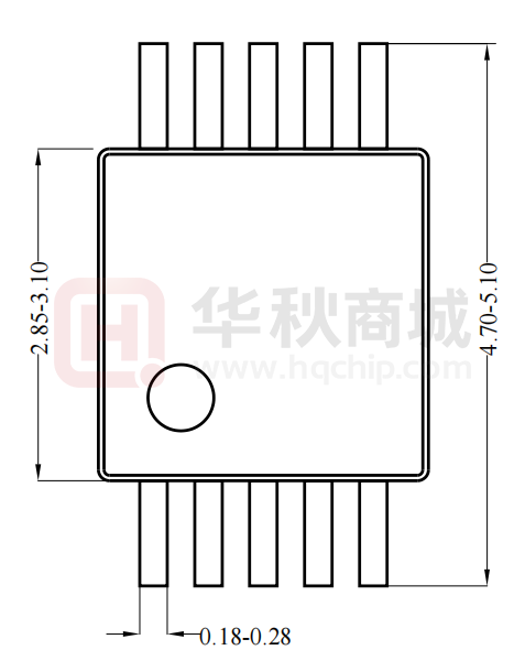
0.10-0.25
0.40-0.80
0.18-0.28
Top view
0.25 base
4.70-5.10
2.85-3.10
MSO10 Package outline & PCB layout
Side view
0.500
5.300
1.350
0.300
0.75-0.95
0.00-0.15
2.85-3.10
0.50 (TYP)
Notes:
Front view
Recommended Pad Layout
All dimension in millimeter and exclude mold flash & metal burr.
AN_SQ52201 Rev. 0.9
© 2021 Silergy Corp.
Silergy Corp. Confidential- Prepared for Customer Use Only
17
All Rights Reserved.
�AN_SQ52201
Taping & Reel Specification
1. Taping Orientation
MSOP10
Feeding direction
2. Carrier Tape & Reel Specification for Packages
Reel
Size
Package
types
Tape width
(mm)
Pocket
pitch(mm)
Reel size
(Inch)
Trailer
length(mm)
Leader length
(mm)
Qty per
reel
MSOP10
12
8
13"
400
400
3000
3. Others: NA
AN_SQ52201 Rev. 0.9
© 2021 Silergy Corp.
Silergy Corp. Confidential- Prepared for Customer Use Only
18
All Rights Reserved.
�AN_SQ52201
IMPORTANT NOTICE
1. Right to make changes. Silergy and its subsidiaries (hereafter Silergy) reserve the right to change any information
published in this document, including but not limited to circuitry, specification and/or product design, manufacturing or
descriptions, at any time and without notice. This document supersedes and replaces all information supplied prior to the
publication hereof. Buyers should obtain the latest relevant information before placing orders and should verify that such
information is current and complete. All semiconductor products are sold subject to Silergy’s standard terms and conditions of
sale.
2. Applications. Application examples that are described herein for any of these products are for illustrative purposes only.
Silergy makes no representation or warranty that such applications will be suitable for the specified use without further testing or
modification. Buyers are responsible for the design and operation of their applications and products using Silergy products.
Silergy or its subsidiaries assume no liability for any application assistance or designs of customer products. It is customer’s sole
responsibility to determine whether the Silergy product is suitable and fit for the customer’s applications and products planned.
To minimize the risks associated with customer’s products and applications, customer should provide adequate design and
operating safeguards. Customer represents and agrees that it has all the necessary expertise to create and implement safeguards
which anticipate dangerous consequences of failures, monitor failures and their consequences, lessen the likelihood of failures
that might cause harm and take appropriate remedial actions. Silergy assumes no liability related to any default, damage, costs or
problem in the customer’s applications or products, or the application or use by customer’s third-party buyers. Customer will
fully indemnify Silergy, its subsidiaries, and their representatives against any damages arising out of the use of any Silergy
components in safety-critical applications. It is also buyers’ sole responsibility to warrant and guarantee that any intellectual
property rights of a third party are not infringed upon when integrating Silergy products into any application. Silergy assumes no
responsibility for any said applications or for any use of any circuitry other than circuitry entirely embodied in a Silergy product.
3. Limited warranty and liability. Information furnished by Silergy in this document is believed to be accurate and reliable.
However, Silergy makes no representation or warranty, expressed or implied, as to the accuracy or completeness of such
information and shall have no liability for the consequences of use of such information. In no event shall Silergy be liable for
any indirect, incidental, punitive, special or consequential damages, including but not limited to lost profits, lost savings, business
interruption, costs related to the removal or replacement of any products or rework charges, whether or not such damages are
based on tort or negligence, warranty, breach of contract or any other legal theory. Notwithstanding any damages that customer
might incur for any reason whatsoever, Silergy’ aggregate and cumulative liability towards customer for the products described
herein shall be limited in accordance with the Standard Terms and Conditions of Sale of Silergy.
4. Suitability for use. Customer acknowledges and agrees that it is solely responsible for compliance with all legal, regulatory
and safety-related requirements concerning its products, and any use of Silergy components in its applications, notwithstanding
any applications-related information or support that may be provided by Silergy. Silergy products are not designed, authorized or
warranted to be suitable for use in life support, life-critical or safety-critical systems or equipment, nor in applications where
failure or malfunction of an Silergy product can reasonably be expected to result in personal injury, death or severe property or
environmental damage. Silergy assumes no liability for inclusion and/or use of Silergy products in such equipment or
applications and therefore such inclusion and/or use is at the customer’s own risk.
5. Terms and conditions of commercial sale. Silergy products are sold subject to the standard terms and conditions of
commercial sale, as published at http://www.silergy.com/stdterms, unless otherwise agreed in a valid written individual
agreement specifically agreed to in writing by an authorized officer of Silergy. In case an individual agreement is concluded only
the terms and conditions of the respective agreement shall apply. Silergy hereby expressly objects to and denies the application
of any customer’s general terms and conditions with regard to the purchase of Silergy products by the customer.
6. No offer to sell or license. Nothing in this document may be interpreted or construed as an offer to sell products that is
open for acceptance or the grant, conveyance or implication of any license under any copyrights, patents or other industrial or
intellectual property rights. Silergy makes no representation or warranty that any license, either express or implied, is granted
under any patent right, copyright, mask work right, or other intellectual property right. Information published by Silergy
regarding third-party products or services does not constitute a license to use such products or services or a warranty or
endorsement thereof. Use of such information may require a license from a third party under the patents or other intellectual
property of the third party, or a license from Silergy under the patents or other intellectual property of Silergy.
For more information, please visit: www.silergy.com
© 2021 Silergy Corp.
AN_SQ52201 Rev. 0.9
© 2021 Silergy Corp.
All Rights Reserved.
Silergy Corp. Confidential- Prepared for Customer Use Only
19
All Rights Reserved.
�