Application Note: SY56805A1
PoE Power Device
General Description
Features
The SY56805A1 is a combined Power over Ethernet
(PoE) powered device (PD) interface and primary side
converter optimized specifically for isolated converter
designs. The PoE interface supports the IEEE 802.3af
standard as a 13W Type 1 powered device.
•
•
•
•
•
•
•
•
•
•
SY56805A1 features a detection signature pin which can
also be used to disable the internal hotswap MOSFET.
This allows the PoE function to be turned off during
powered operation. Classification can be programmed to
any of the defined Type 1 PD with a single resistor.
D1
CIN
VDD
COUT1
VCC
CLS
DRAIN
VSS
VOUT
RVC1 DVC1
RZCS1
ZCS
APD
RZCS2
SOURCE
RCS1
CS
RCS2
RTN
CVC
RCLS
yC
Sil
D2
RAPD2
Adapter
RO
N
.C
orp
T1
DA
RAPD1
dF
de
nti
a
Note
----
DEN
erg
From Ethernet
Pairs 4-5,7-8
C1
Z1
RDEN
From Ethernet
Pairs 1-2,3-6
Typical Applications
IEEE 802.3af Compliant Devices
Video and VoIP Telephones
RFID Readers
Multiband Access Points
Security Cameras
on
fi
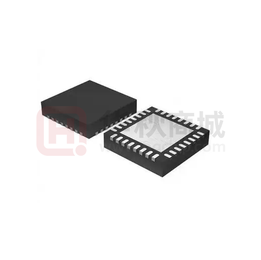
Package type
QFN5*5-32L
•
•
•
•
•
lP
SY56805 □(□□)□
Ordering Number
SY56805A1QEC
Applications
rep
are
Ordering Information
Temperature Code
Package Code
Optional Spec Code
IR
IT
or
K
To achieve higher efficiency and better EMI
performance, SY56805A1 drives Flyback converters in
the Quasi-Resonant mode and adaptive PWM/PFM
control. The flyback converter integrate a 150V, 0.14Ω
MOSFET.
Power Up to 13W(input) PDs
Supports the IEEE 802.3af Standard
Primary Side Control
QR-mode Operation for High Efficiency
PWM/PFM Control for Higher Average Efficiency
Adapter ORing Support
100 V, 0.45Ω Hotswap MOSFET
Integrate 150V, 0.14Ω MOSFET for Converter
RoHS Compliant and Halogen Free
Compact Package: QFN5*5-32L
Figure 1. Schematic Diagram
AN_SY56805A1 Rev.0.9B
© 2022 Silergy Corp.
Silergy Corp. Confidential- Prepared for Customer Use Only
All Rights Reserved.
1
�AN_SY56805A1
NC
NC
26
25
1
24
RTN
NC
2
23
RTN
VSS
3
22
RTN
21
NC
20
VCC
VSS
Drain
4
Exposed
Pad
5
CLS
6
19
APD
7
18
NC
8
14
15
16
SOURCE
SOURCE
NC
NC
dF
13
SOURCE
12
SOURCE
CS
rep
are
11
10
NC
SOURCE
9
17
NC
ZCS
or
K
DEN
IR
IT
VDD
RO
N
NC
NC
29
NC
NC
30
27
NC
31
28
NC
32
Pinout (top view)
(QFN5*5-32L)
Top Mark: EBFxyz (device code: EBF, x=year code, y=week code, z= lot number code)
Pin
VDD
1
VSS
3,4
DEN
5
CLS
6
Connect a resistor from CLS to VSS to program classification current. 2.5 V is applied to the
program resistor during classification to set class current.
APD
7
Pull APD above 1.5 V disables the internal hotswap switch. This forces power to come from an
external VDD-RTN adapter. Connect APD to RTN when not used.
SOURCE
11,12,13,14
SOURCE
15
de
nti
a
Description
Connect to the positive PoE input power rail. VDD powers the PoE interface circuits. Bypass
with a 0.1 μF capacitor and protect with a TVS.
erg
yC
orp
.C
on
fi
Connect to the negative power rail derived from the PoE source.
Connect a 24.9 kΩ resistor from DEN to VDD to provide the PoE detection signature. Pulling
this pin to VSS during powered operation causes the internal hotswap MOSFET to turn off.
18
Source of the internal power MOSFET.
Internal connected to the source of the internal power MOSFET, this pin can be floating.
Current sense pin.
ZCS
Sil
CS
lP
Name
19
Inductor current zero-crossing detection pin. This pin receives the auxiliary winding voltage by a
resistor divider and detects the inductor current zero crossing point.
VCC
20
DC/DC converter bias voltage.
RTN
22,23,24
Drain
Exposed Pad
NC
others
RTN is the output of the PoE hotswap MOSFET.
Drain of the internal power MOSFET.
Not connected.
AN_SY56805A1 Rev.0.9B
© 2022 Silergy Corp.
Silergy Corp. Confidential- Prepared for Customer Use Only
All Rights Reserved.
2
�AN_SY56805A1
Absolute Maximum Ratings (1)
RO
N
Input voltage range [DEN, VDD, RTN (2)] to VSS --------------------------------------------------------------------- -0.3-100V
Input voltage range [VDD, VCC] to RTN ------------------------------------------------------------------------------- -0.3-100V
Input voltage range CLS (3) to VSS--------------------------------------------------------------------------------------- -0.3- 5.5V
Input voltage range [ZCS, CS, APD] to RTN -------------------------------------------------------------------------- -0.3- 5.5V
Package Thermal Resistance (4)
QFN5*5-32L, θJA ----------------------------------------------------------------------------------------------- 25.13°C/W
QFN5*5-32L, θJC ----------------------------------------------------------------------------------------------- 16.85°C/W
Junction Temperature Range ------------------------------------------------------------------------------------ ---- -45°C to 150°C
Lead Temperature (Soldering, 10 sec.) --------------------------------------------------------------------------------------- 260°C
Storage Temperature Range ---------------------------------------------------------------------------------------- -65°C to 150°C
IR
IT
Recommended Operating Conditions
or
K
Input voltage range [RTN, VDD] to VSS------------------------------------------------------------------------------------ 0- 72V
Input voltage range VDD to RTN -------------------------------------------------------------------------------------------- 0- 72V
Input voltage range VCC to RTN --------------------------------------------------------------------------------------------- 0- 18V
Junction Temperature Range ---------------------------------------------------------------------------------------- -40°C to 125°C
dF
Notes:
(1): Stresses beyond the “Absolute Maximum Ratings” may cause perm anent damage to the device. These
rep
are
are stress ratings only. Functional operation of the device at these or any other conditions beyond those
indicated in the operational sections of the specification is not implied. Exposure to absolute maximum rating
conditions for extended periods may affect device reliability.
Sil
erg
yC
orp
.C
on
fi
de
nti
a
lP
(2): IRTN=0 for VRTN>80V.
(3): Do not apply voltage to this pin.
(4): JESD 51-2,-5,-7,-8,-14 standard.
AN_SY56805A1 Rev.0.9B
© 2022 Silergy Corp.
Silergy Corp. Confidential- Prepared for Customer Use Only
All Rights Reserved.
3
�AN_SY56805A1
Block Diagram
VCC
VDD
Control
VO
Estimator
ZCS_FB
RO
N
ZCS
Valley_DET
enb
ZCS_OVP
VCC_OVP
IR
IT
Valley
Detect
ZCS_OVP
COMP
gm
Protection
IPK_SEN
CS
Drain
Flimit_SET
COMP Behavior
(Frequency_ set、
Ipk_set)
IPK_SET
rep
are
Soft start
dF
Valley_DET
or
K
ZCS_REF
PWM
generator
PWM
SOURCE
IPK_Sense
de
nti
a
lP
IPK_Sense
Detection
VSS
DEN
Classification
Logic&
Regulator
CLS
Control logic
& Inrush and
current limit
APD
Sil
erg
yC
orp
.C
on
fi
VDD
VSS
AN_SY56805A1 Rev.0.9B
© 2022 Silergy Corp.
Current
sense
RTN
Silergy Corp. Confidential- Prepared for Customer Use Only
All Rights Reserved.
4
�AN_SY56805A1
Electrical Characteristics
(Unless otherwise noted: CVCC=0.1 μF, RDEN=24.9 kΩ, RCLS open, VVDD-VVSS = 48 V, 9 V ≤ VCC≤ 18 V. Typical
specifications are at 25°C.)
DC-DC Controller Section
IVCC
VDD=48V, VCC=0V
VZCS_OVP
Blanking Time for OFF Time
TOFF_MIN
CS
Maximum Threshold Voltage
VLIMIT
dF
ZCS OVP Threshold
Max OFF Time
TOFF_MAX
Maximum Switching Frequency
FMAX
INTEGRATED MOSFET
VBV
RDSON
VGS=12V,IDS=0.1A
VAPD_EN
.C
VAPD rising
VAPD_H
Hysteresis
orp
yC
APD Threshold Voltage
APD Leakage Current
VGS=0V,IDS=250µA
on
fi
Breakdown Voltage
Static Drain-Source OnResistance
APD
de
nti
a
TON_MAX
lP
SWITCHING
Max ON Time
Unit
9.45
200
9
2.5
7
22
280
350
V
V
V
V
µA
0.5
1
2
mA
1.18
1.2
1.22
V
1.35
1.45
1.55
V
0.53
0.64
0.75
µs
0.92
1.06
1.2
V
6.5
Typ
RO
N
VCC falling
rep
are
VZCS_REF
Max
8.55
ZCS
Voltage Reference
Min
IR
IT
Startup Current Source
Conditions
or
K
VSS=RTN, all voltages referred to RTN.
Parameter
Symbol
VCC
VCC Turn-on Threshold
VVCC_ON
VCC UVLO Hysteresis
VVCC_HYS
VCC SCP Threshold
VVCC_SCP
VCC OVP Voltage
VVCC_OVP
Quiescent Current
IQ
7.5
12
µs
400
550
700
µs
160
200
280
kHz
150
V
Ω
0.14
1.4
1.5
1.6
V
0.3
VAPD=5.5V
V
1
μA
erg
THERMAL SHUTDOWN
Thermal Shutdown Temperature
150
°C
20
°C
Sil
Hysteresis
TJ rising
AN_SY56805A1 Rev.0.9B
© 2022 Silergy Corp.
Silergy Corp. Confidential- Prepared for Customer Use Only
All Rights Reserved.
5
�AN_SY56805A1
PD Interface Section
All voltages referred to VSS unless otherwise noted
Symbol
DEN
Detection Current
Detection Bias Current
VPD_DIS
ICLS
Classification Regulator Lower
Threshold
Classification Regulator Upper
Threshold
HOTSWAP MOSFET
On Resistance
VCL_ON
VCL_H
VCU_OFF
VCU_H
or
K
Classification Current
dF
CLS
lP
Current Limit
de
nti
a
Inrush Limit
Leakage Current
Min
Typ
7
10
μA
3
4
0.1
5
5
V
μA
2
10
18
28
40
11
2
22
0.6
13
3
23
1
mA
mA
mA
mA
mA
V
V
V
V
0.45
0.6
Ω
9
1
21
0.3
580
50
60
Thermal Shutdown Temperature
mA
40
μA
36
V
Hysteresis
4.3
V
TJ rising
150
°C
20
°C
Sil
erg
yC
35
80
VUVLO_H
orp
Hysteresis
34
mA
VDD rising
on
fi
THERMAL SHUTDOWN
μA
μA
VUVLO_R
.C
UVLO Threshold
Unit
4.5
VVDD=VRTN=100V, DEN=VSS
UVLO
Max
60
400
IR
IT
VDEN=VVDD=57V,measure IDEN
VDD= RTN=VSUPPLY positive
RCLS=1270Ω
RCLS=243Ω
RCLS=137Ω
RCLS=90.9Ω
RCLS=63.4Ω
Regulator turns on, VDD rising
Hysteresis
Regulator turns off, VDD rising
Hysteresis
rep
are
Hotswap Disable Threshold
DEN Leakage Current
CLASSIFICATION
Conditions
VVDD= RTN=VSUPPLY positive
VVDD=1.6V
VVDD=10V
VVDD=10V,float DEN, measure
ISUPPLY
RO
N
Parameter
DETECTION
AN_SY56805A1 Rev.0.9B
© 2022 Silergy Corp.
Silergy Corp. Confidential- Prepared for Customer Use Only
All Rights Reserved.
6
�AN_SY56805A1
Typical Performance Characteristics
(Test condition: input voltage: 37-57Vdc; output spec: 12Vdc/1A; Ambient temperature: 25±5 ℃; Ambient
humidity:65±25%.)
Startup
Shutdown
(VIN=37V(DC)@Full Load)
(VIN=37V(DC)@Full Load)
20V/div
VBUS
20V/div
VOUT
12V/div
VOUT
12V/div
ISEN
1V/div
ISEN
1V/div
IR
IT
IOUT
1A/div
dF
Time (10ms/div)
Startup
VOUT
12V/div
ISEN
1V/div
1A/div
Shutdown
VBUS
VOUT
12V/div
ISEN
1V/div
IOUT
Time (10ms/div)
orp
Steady
Steady
ISEN
1V/div
IOUT
erg
12V/div
Sil
VOUT
yC
(VIN=37V(DC)@Full Load)
50V/div
1A/div
Time (4µs/div)
AN_SY56805A1 Rev.0.9B
© 2022 Silergy Corp.
1A/div
.C
Time (10ms/div)
Time (10ms/div)
(VIN=57V(DC)@Full Load)
20V/div
on
fi
IOUT
lP
20V/div
de
nti
a
VBUS
rep
are
(VIN=57V(DC)@Full Load)
VDrain
1A/div
or
K
IOUT
RO
N
VBUS
(VIN=57V(DC)@Full Load)
VDrain
50V/div
VOUT
12V/div
ISEN
1V/div
IOUT
1A/div
Time (4µs/div)
Silergy Corp. Confidential- Prepared for Customer Use Only
All Rights Reserved.
7
�AN_SY56805A1
Short Circuit Protection
Short Circuit Protection
(VIN=37V(DC)@Full Load)
(VIN=57V(DC)@Full Load)
50V/div
VDrain
50V/div
VOUT
12V/div
VOUT
12V/div
ISEN
1V/div
ISEN
1V/div
IR
IT
IOUT
1A/div
IOUT
Line Regulation
dF
37V
48V
57V
12.03
VIN=37V
VIN=48V
VIN=57V
11.97
11.90
0%
25%
50%
75%
100%
Output Current Rate(%)
Sil
erg
yC
orp
.C
on
fi
Input Voltage (V)
Output Voltage (V)
11.97
12.10
rep
are
I=0A
I=0.25A
I=0.5A
I=0.75A
I=1A
lP
12.03
de
nti
a
Output Voltage (V)
Load Regulation
12.16
12.10
11.90
1A/div
Time (1s/div)
or
K
Time (1s/div)
12.16
RO
N
VDrain
AN_SY56805A1 Rev.0.9B
© 2022 Silergy Corp.
Silergy Corp. Confidential- Prepared for Customer Use Only
All Rights Reserved.
8
�AN_SY56805A1
voltage across hotswap switch is sufficiently low,
indicating the switcher supply capacitor is almost
completely charged. Once the inrush current falls and
the RTN drops to nearly zero, the PD current limit
switches to the operational level.
Operation Principles
Protocol Section
Detection
In order to identify a device as a valid PD, the Power
Sourcing Equipment (PSE) senses the Ethernet
connection by applying two voltages in a range of 2.8
V to 10 V on the Ethernet cable and measuring the
corresponding currents. An equivalent resistance is
calculated using the ΔV/ΔI. During this phase, the PD
must present a resistance between 23.75 kΩ and 26.25
kΩ. The value of the detection resistance has to be
selected also taking into account the typical drop in
voltage of the diode bridges. The typical value that can
be used in most case is 24.9 kΩ.
Adapter Power Input
IR
IT
RO
N
In some applications, it is desirable to power the PD
from an auxiliary power source such as a wall adapter.
The SY56805A1 supports forced operation from either
of the power sources. Figure 1 illustrates the
recommended connection of the adapter power to PD.
The hot-swap switch is disabled while the adapter is
used to pull APD high (up to 1.5V), blocking the PoE
source from powering the output.
RDEN
de
nti
a
on
fi
Power at
PD(W)
Class
current
(mA)
Resistor
0
0.44~12.95
0~4
1270
1
0.44~3.84
9~12
243
2
3.84~6.49
137
3
erg
17~20
6.49~12.95
26~30
90.9
4
-
36~44
63.4
yC
orp
Class
Sil
.C
Table 1. Class Resistor Selection
Inrush and Operational Current Limit
VDD
DEN
RCLS
CLS
VSS
RTN
APD
Adapter
RAPD1
rep
are
dF
From PSE
lP
In the classification mode, the PSE will classify the PD
for one of five power levels or classes. This allows the
PSE to efficiently manage power distribution. The five
different classes is shown in Table 1, it determine the
class the PD must advertise. An external resistor (RCLS)
connected from CLS to VSS sets the classification
current. The PSE may disconnect a PD if it draws more
than its stated Class power. During hardware
Classification, the PSE presents a fixed voltage
between 15.5 V and 20.5 V to the PD, which in turn
draws a fixed current set by RCLS. PD current is
measured by the PSE to determine which of the five
available classes is advertised (see Table 1). The
SY56805A1 disables classification while the input
voltage is above 22V to avoid excessive power
dissipation. If the PD thermal limit is trigger or when
APD or DEN is active, the CLS reference voltage will
be turned off .
or
K
Classification
RAPD2
Fig.1 Adapter Power Input
DC-DC Controller Operation
Start-up Operation
After DC supply is powered on, the rectified BUS
voltage ramps up. The capacitor across VCC and RTN
pins, CVCC, is charged up by the BUS voltage through
internal start up circuit. Once VVCC rises up to VVCC_ON,
the internal blocks starts the operation. VVCC will
subsequently be pulled down by the power
consumption of the circuitry until the auxiliary winding
of Flyback transformer can supply sufficient energy.
To avoid triggering VVCC_SCP threshold during start-up,
the VCC bypass capacitor should be large enough to
maintain VVCC above VVCC_SCP(7V typical). The startup procedure is divided into two sections, as shown in
Fig.2: tSTC is the CVCC charged up section, and tSTO is
the output voltage built-up section. The start up time tST
composes of tSTC and tSTO, and usually tSTO is much
smaller than tSTC.
Once the classification is successfully completed, the
PSE will rise its voltage, when the input voltage is
above UVLO turn on threshold(35V), the hotswap
switch is turned on, and the input capacitor is charged
with a low current (inrush current) limit until the
AN_SY56805A1 Rev.0.9B
© 2022 Silergy Corp.
Silergy Corp. Confidential- Prepared for Customer Use Only
All Rights Reserved.
9
�AN_SY56805A1
N AUX
(1)
NS
NAUX is the turns of auxiliary winding; NS is the turns
of secondary winding; VD_F is the forward voltage of
the power diode.
VAUX = (VOUT + VD _ F )
Fig.2 Start up
Quasi-Resonant Operation
IR
IT
RO
N
At the current zero-crossing point, VD_F is nearly zero,
so VOUT is proportional with VAUX exactly. The voltage
of this point is sampled by the IC as the feedback of
output voltage. The resistor divider is designed by
VZCS _ REF
R ZCSD
N
=
AUX (2)
VOUT
R ZCSU + R ZCSD
NS
Where VZCS_REF is the internal voltage reference.
QR mode operation provides low turn-on switching
losses for Flyback converter.
VNAUX
IPP
dF
IPRI
or
K
VG
rep
are
Valley
VDS
ISP
ISEC
IOUT
tDIS
de
nti
a
Fig.3 QR mode operation
lP
tS
.C
on
fi
The voltage across drain and source of the primary
MOSFET is reflected by the auxiliary winding of the
Flyback transformer. ZCS pin detects the voltage
across the auxiliary winding by a resistor divider.
When the voltage across drain and source of the
primary MOSFET is at voltage valley, the MOSFET
would be turned on.
Output Voltage Control
yC
orp
In order to achieve primary side constant voltage
control, the output voltage is detected by the auxiliary
winding voltage.
RAUX
CVCC
Sil
RZCSD
erg
NAUX
RZCSU
VCC
SY56805A1
ZCS
Fig.4 ZCS pin connection
As shown in Fig.5, during OFF time, the voltage across
the auxiliary winding is
AN_SY56805A1 Rev.0.9B
© 2022 Silergy Corp.
VAUX
VOUT
t1
tS
t2
N AUX
NS
t3
Fig.5 Auxiliary winding voltage waveforms
Fault Protection Modes
ZCS Pin Short Protection
The SY56805A1 has a protection against faults caused
by a shorted ZCS pin. During start-up, the voltage on
the ZCS pin is monitored. In normal situations, the
voltage on the ZCS pin reaches the sense protection
trigger level. When the ZCS voltage does not reach this
level, the ZCS pin is shorted and the protection is
activated. The IC stops switching and discharge the
VCC voltage. Once VVCC is below VVCC_OFF, the IC
will shut down and be charged again by VDD.
CS pin Short Protection
The SY56805A1 has a protection against the faults
caused by shorting CS pin to RTN. During start-up, the
voltage on the CS pin is monitored. If the VCS does not
Silergy Corp. Confidential- Prepared for Customer Use Only
All Rights Reserved.
10
�AN_SY56805A1
exceed 150mV after 2.5µS, the protection will be
triggered, the IC stops switching and discharge the
VCC voltage. Once VVCC decreases below VVCC_OFF,
the IC will shut down and the VCC will be charged
again by VDD.
Power Device Design
MOSFET and DIODE
When the operation condition is with maximum input
voltage and full load, the voltage stress of MOSFET
and secondary power diode is maximized;
Output Over Voltage Protection
When the ZCS pin signal exceeds 1.45V, reflecting an
output over-voltage condition, SY56805A1 will stop
switching and discharge the VCC voltage. Once VVCC
is below VVCC_OFF, the IC will shut down and the VCC
will be charged again by VDD.
VD_R_MAX =
IR
IT
or
K
When the operation condition is with minimum input
voltage and full load, the current stress of MOSFET
and power diode is maximized.
I MOS_PK_MAX =IP_PK_MAX (5)
dF
yC
orp
.C
on
fi
de
nti
a
lP
The SCP will be triggered when the VCC is falling
below VVCC-SCP (7V typical) and the voltage of internal
comp is up to 2V.
When the IC starts up with heavy load, or the output
current is getting heavier and heavier during normal
operation, or output is shorted to ground, the VCC
voltage will decrease and internal COMP will be high,
Once VVCC is below VVCC_SCP, IC will shut down
immediately, VCC will be charged again by VDD. To
avoid thermal rising risk, a digital counter is adopted.
When VCC has reached VVCC_ON, the counter will plus
1. When the counter has reached number 8, SCP flag
signal will be reset. Meanwhile, IC will try to start up
again.
In order to guarantee SCP function is not affected by
voltage spike of auxiliary winding, a filter resistor
RAUX is needed.
erg
+VOUT (4)
rep
are
Short Circuit Protection (SCP)
I MOS_RMS_MAX =I P_RMS_MAX (6)
I D_PK_MAX =N PS I P_PK_MAX (7)
I D_AVG =I OUT (8)
Where IP_PK_MAX and IP_RMS_MAX are maximum
primary peak current and RMS current, which will be
introduced later.
Transformer (NPS and LM)
NPS is limited by the electrical stress of the power
MOSFET:
VMOS_(BR)DS 90%-VDC_MAX -ΔVS
(9)
NPS
VOUT +VD_F
Where VMOS_(BR)DS is the breakdown voltage of the
power MOSFET.
VCC
CVCC
SY56805A1
In Quasi-Resonant mode, each switching period cycle
tS consists of three parts: current rising time t1, current
falling time t2 and quasi-resonant time t3 shown in
Fig.8.
Sil
NAUX
N PS
Where VDC_MAX is maximum input DC voltage; NPS is
the turns ratio of the Flyback transformer; V OUT is the
rated output voltage; VD_F is the forward voltage of
secondary power diode; ΔVS is the overshoot voltage
clamped by RCD snubber during OFF time.
VCC Over Voltage Protection
When the VCC voltage exceeds VVCC_OVP threshold,
SY56805A1 will stop switching and discharge the
VCC voltage. Once VVCC is below VVCC_OFF, the
SY56805A1 will shut down and the VCC will be
charged again by VDD.
RAUX
VDC_MAX
RO
N
VMOS_DS_MAX =VDC_MAX +N PS (VOUT +VD_F )+ΔVS (3)
Fig. 6 Filter resistor RAUX
AN_SY56805A1 Rev.0.9B
© 2022 Silergy Corp.
Silergy Corp. Confidential- Prepared for Customer Use Only
All Rights Reserved.
11
�AN_SY56805A1
VG
t1 =
t2 =
IPP
IPRI
L M I P _ PK _ MAX
tS =
ISEC
(14)
1
(15)
fS _ MIN
current
IR
IT
VDS
or
K
t3
t2
tS
(f) Compute secondary maximum peak current
IS_PK_MAX and RMS current IS_RMS_MAX for the
transformer fabrication.
IS_PK_MAX =N PS I P_PK_MAX (17)
dF
t1
Fig.7 switching waveforms
(b) Preset minimum frequency fS_MIN
on
fi
de
nti
a
lP
Once the minimum frequency fS_MIN is set, the
inductance of the transformer could be induced. The
design flow is shown as below:
(a)Select NPS
VMOS_(BR)DS 90%-VDC_MAX -ΔVS
(10)
NPS
VOUT +VD_F
IS _ RMS _ MAX =
rep
are
When the operation condition is with minimum input
DC RMS voltage and full load, the switching frequency
is minimum frequency, the maximum peak current
through MOSFET and the transformer happens.
orp
.C
(c) Compute inductor LM and maximum primary peak
current IP_PK_MAX
yC
2POUT
2POUT
2POUT
+
+
CDrain fS_ MIN
VDC _ MIN NPS (VOUT + VD _ F )
2POUT
I 2P _ PK _ MAX fS _ MIN
(11)
(12)
erg
LM =
N PS (VOUT + VD _ F )
(e) Compute primary maximum RMS
IP_RMS_MAX for the transformer fabrication.
t
3
IP _ RMS _ MAX =
IP _ PK _ MAX 1 (16)
3
tS
IOUT
IP _ PK _ MAX =
LM I P _ PK _ MAX
RO
N
ISP
(13)
VBUS
Transformer Design (NP,NS,NAUX)
The design of the transformer is similar with ordinary
Flyback transformer. the parameters below are
necessary:
Necessary parameters
Turns ratio
Inductance
Primary maximum current
Primary maximum RMS current
Secondary maximum RMS current
Sil
(d) Compute current rising time t1 and current falling
time t2
The design rules are as followed:
(a) Select the magnetic core style, identify the effective
area Ae.
(b) Preset the maximum magnetic flux ΔB
ΔB=0.22~0.26T
NP =
L M I P_PK_MAX
ΔB A e
(19)
(d) Compute secondary turn NS
NS =
© 2022 Silergy Corp.
NPS
LM
IP_PK_MAX
IP_RMS_MAX
IS_RMS_MAX
(c) Compute primary turn NP
Where CDrain is the parasitic capacitance at drain of
MOSFET; η is the efficiency; POUT is rated full load
power.
AN_SY56805A1 Rev.0.9B
t
3
N PS I P _ PK _ MAX 2 (18)
3
tS
NP
(20)
N PS
Silergy Corp. Confidential- Prepared for Customer Use Only
All Rights Reserved.
12
�AN_SY56805A1
Table2. Class Resistor Selection
(e) compute auxiliary turn NAUX
Where VVCC is the working voltage of VCC pin
(10V~15V is recommended).
(f) Select an appropriate wire diameter
With IP_RMS_MAX and IS_RMS_MAX, select appropriate
wire to make sure the current density ranges from
4A/mm2 to 10A/mm2.
1270
1
0.44
3.84
243
2
3.84
6.49
137
3
6.49
12.95
90.9
IR
IT
or
K
dF
lP
de
nti
a
on
fi
(23)
PRCD
The CRCD is related with the voltage ripple of the
snubber ΔVC_RCD:
N (VOUT +VD_F )+ΔVS
(24)
CRCD = PS
R RCD fS ΔVC_RCD
.C
orp
yC
erg
The standard specifies a detection signature resistance,
RDEN between 23.7 kΩ and 26.3 kΩ. Connect a 24.9kΩ
resistor from DEN to VDD to provide the PoE
detection signature.
VDD to VSS ESD Protection
Voltage transients caused by surge or other special
applications can occur, a TVS (D1, see in Fig.8) must
limit this voltage to be within the absolute maximum
ratings. The TVS such as SMBJ58A can be used. A
TVS with negative resistance characteristic is not
recommended. A Schottky diode (D2 on the Fig.8)
such as PT3L100F-A is required between VSS and
RTN for application design.
RDEN
24.9k
VDD
DEN
C1 D1
A resistor from CLS to VSS programs the classification
current per the IEEE standard. The PD power ranges
and corresponding resistor values are listed in
following table. The power assigned should correspond
to the maximum average power drawn by the PD
during operation. SY56805A1 supports class 0-3 power
levels.
Sil
DEN Resistor Selection
CLS
RCLS
From
Ethernet
4-5,7-8
(NPS (VOUT +VD_F )+ΔVS )
2
(22)
R APD1 + R APD2
(VAPDEN - VAPDH)
R APD2
From
Ethernet
1-2,3-6
LK
POUT (22)
LM
rep
are
The RRCD is related with the power loss,
CLS Resistor Selection
12.95
VAPDTR_OFF =
Where NPS is the turns ratio of the flyback transformer;
VOUT is the output voltage; VD_F is the forward voltage
of the power diode; ΔVS is the overshoot voltage
clamped by RCD snubber; LK is the leakage inductor;
LM is the inductance of the Flyback transformer; POUT
is the output power.
R RCD =
0.44
R APD1 = R APD2 (VAPDTR_ON - VAPDEN)/VAPDEN
The power loss of the snubber PRCD is evaluated first
ΔVS
0
APD forces power to come from an external adapter
connected from VDD to RTN by opening the hotswap
switch. Select the APD divider resistors per Equation
(22) where VADPTR_ON is the desired adapter voltage
that enables the APD function as adapter voltage rises.
RCD Snubber for MOSFET
N PS (VOUT +VD_F )+ΔVS
Resistor
APD Resistor Selection
(g) If the winding area of the core and bobbin is not
enough, reselect the core style, go to (a) and redesign
the transformer until the ideal transformer is achieved.
PRCD =
Power at PD
Minmum
Maximum
(W)
(W)
Class
RO
N
V
N AUX =N S VCC (21)
VOUT
SY56805A1
VSS
APD
D2
RTN
Fig.8 VDD to VSS ESD protection
AN_SY56805A1 Rev.0.9B
© 2022 Silergy Corp.
Silergy Corp. Confidential- Prepared for Customer Use Only
All Rights Reserved.
13
�AN_SY56805A1
Input Bypass Capacitor Selection
3
The standard specifies an input bypass capacitor of
0.05 μF to 0.12 μF. Typically a 0.1 μF, 100V ceramic
capacitor between VDD and VSS(C1 on the Fig.8) is
used while the input power source is only PSE (C2 not
connnect).
1
5
4
2
7
Ground ①: ground of BUS capacitor.
Ground ②: ground of bias supply capacitor.
Ground ③: ground node of auxiliary winding.
Ground ④: ground node of divider resistor.
Ground ⑤: primary ground node of Y capacitor.
Ground ⑥: ground node of current sample resistor.
Ground ⑦: ground of IC GND.
IR
IT
RO
N
If the external adapter is also used to power the device,
one capacitor C1 between VDD and VSS, and one
capacitor C2 between RTN and VSS is both
recommended to be connected. The typical value of C1
and C2 is both recommended to be 0.047uF/100V.
Layout
rep
are
dF
or
K
(d) bias supply trace should be connected to the bias
supply capacitor first instead of GND pin. The bias
supply capacitor should be put beside the IC.
(e) Loop of ‘Source pin – current sample resistor –
GND pin’ should be kept as small as possible.
(f) The resistor divider connected to ZCS pin is
recommended to be put beside the IC.
de
nti
a
lP
(a) To achieve better EMI performance and reduce line
frequency ripples, the output of the bridge rectifier
should be connected to the BUS line capacitor first,
then to the switching circuit.
(b) The circuit loop of all switching circuit should be
kept small: primary power loop, secondary loop and
auxiliary power loop.
(c) The connection of primary ground is recommended
as:
6
Design Notice
on
fi
Sil
erg
yC
orp
4.
5.
At no load secondary side diode freewheeling time should be more than TOFF_MIN.
VCC voltage prefer to larger than 10V for all conditions.
At heavy load, the peak-to-peak voltage at the ZCS pin should be less than approximately 100mV after.
TOFF_MIN time. This can be guaranteed by decreasing the leakage inductance and using proper RCD snubber.
RZCSU is the upper resistor of the divider. Normally, its value is recommended between 30kΩ~91kΩ.
In order to ensure the loop stability, the output capacitor should be selected properly. On the other hand, switching
frequency ripple should also be considered. If the switching frequency ripple is too large, increase the capacitance
of Cout properly or use low ESR capacitor.
.C
1.
2.
3.
AN_SY56805A1 Rev.0.9B
© 2022 Silergy Corp.
Silergy Corp. Confidential- Prepared for Customer Use Only
All Rights Reserved.
14
�AN_SY56805A1
Design Example
A design example of typical application is shown below step by step.
Design Specification
VDC
IOUT
37V~57V
1A
VOUT
η
12V
82%
IR
IT
#2. Transformer design (NPS, LM)
37V
50V
12W
VDC_MAX
VMOS-(BR)DS
V D_ F
CDrain
60pF
fS_MIN
150kHz
rep
are
(a)Compute turns ratio NPS first
57V
150V
1V
dF
Conditions
VDC_MIN
ΔVS
POUT(max)
or
K
Refer to Power Device Design
N PS
RO
N
#1. Identify design specification
VMOS_(BR)DS 90%-VDC_MAX -ΔVS
VOUT +VD,F
lP
150V 0.9-57V-50V
12V+1V
=2.15
de
nti
a
=
NPS is set to
on
fi
N PS =2
.C
(b)fS,MIN is preset
orp
fS_MIN =150kHz
Sil
erg
yC
(c) Compute inductor LM and maximum primary peak current IP,PK,MAX
2POUT
I P _ PK _M AX =
N PS VO
VDC _ MIN
N PS VO + VDC _ MIN
2 12W
=
2*12V
0.82 (37V
)
2*12V + 37V
= 2.01A
2POUT
LM =
2
I P _ PK _ MAX fS _ MIN
2 12W
0.82 (2.01A)2 150KHz
= 48.78H
=
AN_SY56805A1 Rev.0.9B
© 2022 Silergy Corp.
Silergy Corp. Confidential- Prepared for Customer Use Only
All Rights Reserved.
15
�AN_SY56805A1
Set: LM=48µH
(d) Compute current rising time t1 and current falling time t2
t2 =
LM I P _ PK _ MAX
VDC_ MIN
=
48H 2.01A
= 2.607s
37V
LM I P _ PK _ MAX
N PS (VOUT + VD _ F )
=
48H 2.01A
= 3.711s
2 (12V + 1V)
RO
N
t1 =
IR
IT
t 3 =π LM CDrain =π 48H 60pF=0.168s
or
K
t S = t1 + t 2 + t 3 = 2.607s + 3.711s + 0.168s = 6.486s
(e) Compute primary maximum RMS current IP-RMS-MAX for the transformer fabrication.
dF
t
3
3
2.607s
IP _ PK _ MAX 1 =
2.01A
= 0.736A
3
tS
3
6.486s
rep
are
IP _ RMS _ MAX =
(f) Compute secondary maximum peak current I S-PK-MAX and RMS current IS-RMS-MAX for the transformer fabrication.
IS_PK_MAX =N PS I P_PK_MAX = 2 2.01A = 4.02A
lP
t
3
3
3.711s
IP _ PK _ MAX 2 = 2
2.01A
= 1.756A
3
tS
3
6.486s
de
nti
a
IS _ RMS _ MAX = N PS
#3. Select secondary power diode
.C
NPS
V D_ F
2
1V
orp
Known conditions at this step
VDC_MAX
57V
VOUT
12V
on
fi
Refer to Power Device Design
VD_R_MAX =
VDC_MAX
N PS
+VOUT
Sil
erg
57V
+12V
2
=40.5V
=
yC
Compute the voltage and the current stress of secondary power diode
I D_PK_MAX =N PS I P_PK_MAX =2 2.01A=4.02A
I D_AVG =1A
#4. Set current sense resistor to achieve ideal output current
AN_SY56805A1 Rev.0.9B
© 2022 Silergy Corp.
Silergy Corp. Confidential- Prepared for Customer Use Only
All Rights Reserved.
16
�AN_SY56805A1
Known conditions at this step
NPS
2
VLIMIT
1V
IOUT,LIM
1.3A
The current sense resistor is
VLIMIT
I P _ PK _M AX
RO
N
RS =
1V
2.01A
=0.498Ω
IR
IT
=
Set Rs
or
K
Rs=0.5
dF
#5. Set ZCS pin
Refer to VOUT
Parameters Designed
RZCSU
rep
are
First identify RZCSU need for line regulation.
lP
56kΩ
Conditions
VOUT
RZCSU
NAUX
de
nti
a
Then compute RZCSD
12V
56kΩ
9
VZCS_REF
NS
1.2V
9
on
fi
R ZCSU
56K
=
= 6.8K
VOUT NAUX
12V 9
− 1)
-1 (
(1.2V+0.1) 9
(VZCS_REF +0.1V)NS
.C
R ZCSD =
orp
Set RZCSD
(Note: In consideration of the propagation delay of internal circuit, a 0.1V is added to VZCS_REF for compensation.)
yC
R ZCSD =6.8kΩ
erg
#6. Set DEN pin
Connect a 24.9kΩ resistor from DEN to VDD
Sil
#7. Set CLS pin
Connect a 1.27kΩ resistor from CLS to VSS
#9. Final result
AN_SY56805A1 Rev.0.9B
© 2022 Silergy Corp.
Silergy Corp. Confidential- Prepared for Customer Use Only
All Rights Reserved.
17
�AN_SY56805A1
C4
1nF/250V
C3
1μF/100V
VDD
DEN
VCC
D1
SMBJ58A
T1
50µH/EP13
CLS
DRAIN
R9
D5
PT5V100B 20
C5
C7
0.1µF/25V 10µF/25V
R3
10
RCLS
1.27k
From
Ethernet
4-5,7-8
R2
10
D2
BAV21W
RDEN
24.9k
C1
68nF/100V
R1
20k
ZCS
D4
BAV21W
C6
10µF/25V
C8
10μF/25V
R4
56k
VSS
R5
6.8k
SOURCE
APD
D3
PT3L100F-A
C10
220μF/16V
R7
1
R8
1
-
Vout
+
or
K
R6
100
IR
IT
RTN
C11
470pF/100V
R10
1k
CS
RAPD
0
C9
10μF/25V
RO
N
From
Ethernet
1-2,3-6
C2
22μF/63V
Sil
erg
yC
orp
.C
on
fi
de
nti
a
lP
rep
are
dF
Fig.9 Design example VIN=37V-57V, PoE application, Vout=12V@1A
AN_SY56805A1 Rev.0.9B
© 2022 Silergy Corp.
Silergy Corp. Confidential- Prepared for Customer Use Only
All Rights Reserved.
18
�AN_SY56805A1
or
K
IR
IT
RO
N
QFN5x5-32L Package outline & PCB Layout
Bottom View
PCB layout (Recommended)
All dimension in millimeter and exclude mold flash & metal burr.
Sil
Notes:
erg
yC
Side View
orp
.C
on
fi
de
nti
a
lP
rep
are
dF
Top View
AN_SY56805A1 Rev.0.9B
© 2022 Silergy Corp.
Silergy Corp. Confidential- Prepared for Customer Use Only
All Rights Reserved.
19
�AN_SY56805A1
Taping & Reel Specification
Feeding direction
or
K
IR
IT
RO
N
1. Taping orientation
de
nti
a
lP
rep
are
dF
2. Carrier Tape & Reel specification for packages
Reel size
(Inch)
Trailer
length(mm)
Leader length
(mm)
Qty per
reel
12
8
13"
400
400
5000
yC
Pocket
pitch(mm)
Sil
QFN5×5
Tape width
(mm)
erg
Package types
orp
.C
on
fi
Reel
Size
3. Others: NA
AN_SY56805A1 Rev.0.9B
© 2022 Silergy Corp.
Silergy Corp. Confidential- Prepared for Customer Use Only
All Rights Reserved.
20
�AN_SY56805A1
Revision History
The revision history provided is for informational purpose only and is believed to be accurate, however, not warranted.
Please make sure that you have the latest revision.
Date
Revision
Change
Revision 0.9B
Update the VVCC_SCP Threshold
April 15, 2021
Revision 0.9A
Update the Package outline & PCB Layout information
October 23, 2020
Revision 0.9
Initial Release
Sil
erg
yC
orp
.C
on
fi
de
nti
a
lP
rep
are
dF
or
K
IR
IT
RO
N
April 2, 2022
AN_SY56805A1 Rev.0.9B
© 2022 Silergy Corp.
Silergy Corp. Confidential- Prepared for Customer Use Only
All Rights Reserved.
21
�AN_SY56805A1
IMPORTANT NOTICE
1. Right to make changes. Silergy and its subsidiaries (hereafter Silergy) reserve the right to change any information published in
this document, including but not limited to circuitry, specification and/or product design, manufacturing or descriptions, at any time
and without notice. This document supersedes and replaces all information supplied prior to the publication hereof. Buyers should
obtain the latest relevant information before placing orders and should verify that such information is current and complete. All
semiconductor products are sold subject to Silergy’s standard terms and conditions of sale.
or
K
IR
IT
RO
N
2. Applications. Application examples that are described herein for any of these products are for illustrative purposes only.
Silergy makes no representation or warranty that such applications will be suitable for the specified use without further testing or
modification. Buyers are responsible for the design and operation of their applications and products using Silergy products. Silergy
or its subsidiaries assume no liability for any application assistance or designs of customer products. It is customer’s sole
responsibility to determine whether the Silergy product is suitable and fit for the customer’s applications and products planned. To
minimize the risks associated with customer’s products and applications, customer should provide adequate design and operating
safeguards. Customer represents and agrees that it has all the necessary expertise to create and implement safeguards which
anticipate dangerous consequences of failures, monitor failures and their consequences, lessen the likelihood of failures that might
cause harm and take appropriate remedial actions. Silergy assumes no liability related to any default, damage, costs or problem in the
customer’s applications or products, or the application or use by customer’s third-party buyers. Customer will fully indemnify
Silergy, its subsidiaries, and their representatives against any damages arising out of the use of any Silergy components in safetycritical applications. It is also buyers’ sole responsibility to warrant and guarantee that any intellectual property rights of a third party
are not infringed upon when integrating Silergy products into any application. Silergy assumes no responsibility for any said
applications or for any use of any circuitry other than circuitry entirely embodied in a Silergy product.
lP
rep
are
dF
3. Limited warranty and liability. Information furnished by Silergy in this document is believed to be accurate and reliable.
However, Silergy makes no representation or warranty, expressed or implied, as to the accuracy or completeness of such information
and shall have no liability for the consequences of use of such information. In no event shall Silergy be liable for any indirect,
incidental, punitive, special or consequential damages, including but not limited to lost profits, lost savings, business interruption,
costs related to the removal or replacement of any products or rework charges, whether or not such damages are based on tort or
negligence, warranty, breach of contract or any other legal theory. Notwithstanding any damages that customer might incur for any
reason whatsoever, Silergy’ aggregate and cumulative liability towards customer for the products described herein shall be limited in
accordance with the Standard Terms and Conditions of Sale of Silergy.
on
fi
de
nti
a
4. Suitability for use. Customer acknowledges and agrees that it is solely responsible for compliance with all legal, regulatory and
safety-related requirements concerning its products, and any use of Silergy components in its applications, notwithstanding any
applications-related information or support that may be provided by Silergy. Silergy products are not designed, authorized or
warranted to be suitable for use in life support, life-critical or safety-critical systems or equipment, nor in applications where failure
or malfunction of an Silergy product can reasonably be expected to result in personal injury, death or severe property or
environmental damage. Silergy assumes no liability for inclusion and/or use of Silergy products in such equipment or applications
and therefore such inclusion and/or use is at the customer’s own risk.
orp
.C
5. Terms and conditions of commercial sale. Silergy products are sold subject to the standard terms and conditions of
commercial sale, as published at http://www.silergy.com/stdterms, unless otherwise agreed in a valid written individual agreement
specifically agreed to in writing by an authorized officer of Silergy. In case an individual agreement is concluded only the terms and
conditions of the respective agreement shall apply. Silergy hereby expressly objects to and denies the application of any customer’s
general terms and conditions with regard to the purchase of Silergy products by the customer.
erg
yC
6. No offer to sell or license. Nothing in this document may be interpreted or construed as an offer to sell products that is open for
acceptance or the grant, conveyance or implication of any license under any copyrights, patents or other industrial or intellectual
property rights. Silergy makes no representation or warranty that any license, either express or implied, is granted under any patent
right, copyright, mask work right, or other intellectual property right. Information published by Silergy regarding third-party
products or services does not constitute a license to use such products or services or a warranty or endorsement thereof. Use of such
information may require a license from a third party under the patents or other intellectual property of the third party, or a license
from Silergy under the patents or other intellectual property of Silergy.
Sil
For more information, please visit: www.silergy.com
© 2022 Silergy Corp.
AN_SY56805A1 Rev.0.9B
© 2022 Silergy Corp.
Powered by TCPDF (www.tcpdf.org)
All Rights Reserved.
Silergy Corp. Confidential- Prepared for Customer Use Only
All Rights Reserved.
22
�