Application Notes: AN_SY6018
Analog Class-D Audio IC
Features
•
•
•
The SY6018 advanced oscillator/PLL circuit employs a
multiple switching frequency option to avoid AM/AF
interferences; this is achieved together with an option
of Master and Slave synchronization, making it
possible to synchronize multiple devices.
•
•
•
•
•
de
nti
a
lP
The SY6018 is fully protected against faults including
short circuit, over temperature, DC error, under voltage
and over voltage. The short circuit, over temperature
and DC error protection includes an auto-recovery
feature. The under voltage and over voltage protection
with hysteresis can be self-cleared.
rep
are
•
Ordering Information
on
fi
SY6018 □(□□)□
orp
Package type
QFN5×5-32
Note
•
•
Applications
•
•
•
•
•
•
•
Flat Panel Display TVs
DLP® TVs
CRT TVs
Powered Speakers
Music Instruments
Boom Box
Consumer Audio Applications
Sil
erg
yC
Ordering Number
SY6018QEC
.C
Temperature Code
Package Code
Optional Spec Code
RO
N
•
IR
IT
•
2×30W into 8Ω BTL Loads @ 10% THD+N from
a 24V Supply
60W into a 4Ω PBTL Load @ 10% THD+N from
a 24V Supply
Wide Voltage Range: 5.6V to 26V
Filter-free Operation
Differential and Single-ended Inputs
Internal Feedback Control with High PSRR
High Efficiency Class-D Operation Eliminates
Need for Heat Sinks
AM/AF Avoidance
Master and Slave Synchronization
Four Fixed-gain Controlled: 20dB, 26dB, 32dB
and 36dB
Selectable BD Mode and 1SPW Mode
Modulation
Integrated Protection Circuits Including Over
Voltage, Under Voltage, Over Temperature, DC
Error, and Short Circuit
Comprehensive Click and Pop Suppression
Space-saving Surface Mount 32Pin QFN
5mm×5mm Package
or
K
•
The SY6018 is a Class-D audio power amplifier with
analog input and high-power efficiency for driving
bridge-tied stereo speakers with up to 2×30W/8Ω or a
bridge-tied mono speaker with up to 60W/4Ω. The
efficiency of the SY6018 eliminates the need for an
external heat sink when playing music.
dF
General Description
AN_SY6018 Rev.0.9D
© 2021 Silergy Corp.
Silergy Corp. Confidential-prepared for Customer Use Only
1
All Rights Reserved.
�AN_ SY6018
Typical Applications
SY6018
AVDD
PVDD
AGND
LINP
Left Channel Negative
LINN
Right Channel Positive
RINP
Right Channel Negative
RINN
GREG
PGND
BSPL
OUTPL
OUTNL
VREF
Shutdown Control
Fault Dectect
Gain & Master/Slave Selection
Mute Control
BSNL
MODSEL
SDZ
BSPR
or
K
BD/1SPW Selection
FAULTZ
OUTPR
GAIN/SLV
dF
MUTE
OUTNR
AM2
AM1
AM0
Synchronizing to Class-D Devices
BSNR
SYNC
rep
are
AM/FM Avoidance Control
RO
N
Left Channel Positive
5.6V to 26V
IR
IT
5.6V to 26V
GREG
lP
(a) Stereo Class-D Amplifier with BTL Output
AVDD
PVDD
AGND
PGND
LINP
BSPL
LINN
OUTPL
on
fi
5.6V to 26V
de
nti
a
SY6018
RINP
Left Channel Negative
RINN
orp
.C
Left Channel Positive
GREG
yC
BD/1SPW Selection
Shutdown Control
erg
Fault Dectect
Gain & Master/Slave Selection
Sil
Mute Control
AM/FM Avoidance Control
Synchronizing to Class-D Devices
5.6V to 26V
OUTNL
VREF
BSNL
MODSEL
SDZ
FAULTZ
BSPR
OUTPR
GAIN/SLV
MUTE
AM2
AM1
AM0
OUTNR
BSNR
GREG
SYNC
(b) Mono Class-D Amplifier with PBTL Output
Fig.1 Typical Application Circuit
AN_SY6018 Rev.0.9D
© 2021 Silergy Corp.
Silergy Corp. Confidential-prepared for Customer Use Only
2
All Rights Reserved.
�AN_ SY6018
OUTPR
29
28
27
26
25
VREF
1
24 PGND
GREG
2
23 OUTNR
GAIN/SLV
3
22 BSNR
AGND
4
LINN
5
20 MODSEL
21 PGND
IR
IT
THERMAL PAD
RO
N
BSPR
30
PVDD
FAULTZ
31
SDZ
RINP
32
PVDD
RINN
Pinout (top view)
6
19 BSNL
7
18 OUTNL
AM2
8
17 PGND
13
14
15
16
PVDD
BSPL
OUTPL
rep
are
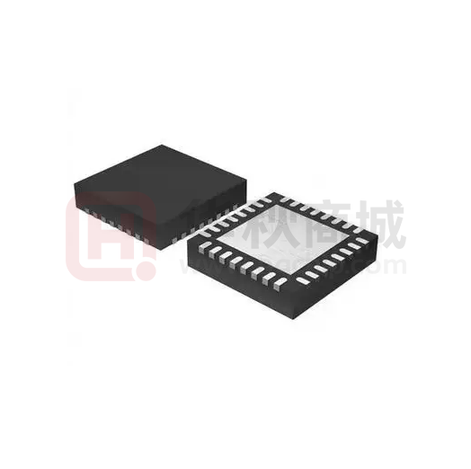
(QFN5×5-32)
dF
12
PVDD
AM0
AM1
11
AVDD
10
SYNC
9
or
K
LINP
MUTE
Sil
erg
yC
orp
.C
on
fi
de
nti
a
lP
Top Mark: BHLxyz (device code: BHL, x=year code, y=week code, z= lot number code)
Pin Name
Pin Number
Description
VREF
1
Internal reference pin. Connect to GREG directly.
GREG
Gate drive supply. Nominal voltage is 3.4V.
2
Gain & Master/Slave mode selection depending on voltage divider from GREG
GAIN/SLV
3
to GND.
AGND
Analog Ground.
4
LINN
5
Negative audio input for left channel. Biased at 1.7V.
LINP
6
Positive audio input for left channel. Biased at 1.7V.
Mute pin (high=mute, low=unmute), TTL logic levels with compliance to
MUTE
7
AVDD.
AM2
8
AM/AF avoidance frequency selection.
AM1
9
AM/AF avoidance frequency selection.
AM0
10
AM/AF avoidance frequency selection.
Clock input/output for synchronizing other Class-D devices. Determined by
SYNC
11
GAIN/SLV pin.
AVDD
12
Analog power supply. Not internally connected to PVDD.
PVDD
13
Power supply.
PVDD
14
Power supply.
BSPL
15
Bootstrap for left positive channel output.
OUTPL
16
Positive left channel output.
PGND
17
Power Ground.
OUTNL
18
Negative left channel output.
BSNL
19
Bootstrap for left negative channel output.
Mode selection (low=BD, high=1SPW), TTL logic levels with compliance to
MODSEL
20
AVDD.
PGND
21
Power Ground.
BSNR
22
Bootstrap for right negative channel output.
OUTNR
23
Negative right channel output.
PGND
24
Power Ground.
OUTPR
25
Positive left channel output.
AN_SY6018 Rev.0.9D
© 2021 Silergy Corp.
Silergy Corp. Confidential-prepared for Customer Use Only
3
All Rights Reserved.
�AN_ SY6018
26
27
28
SDZ
29
FAULTZ
30
RINP
RINN
Thermal Pad
31
32
33
Bootstrap for right positive channel output.
Power supply.
Power supply.
Shutdown pin (low = enter shutdown, high = exit shutdown). TTL logic levels
with compliance to AVDD.
Open drain output used to display general fault, including SCP, OTP, DCP fault
status (low=fault, high=normal).
Positive audio input for right channel. Biased at 1.7V.
Negative audio input for right channel. Biased at 1.7V.
Connect to GND for best system performance.
RO
N
BSPR
PVDD
PVDD
or
K
IR
IT
Block Diagram
GREG
GREG
OUTPR
RINP
RINN
INPUT
CIRCUIT
Differential Modulation and Compensation
OUTNR
ANTICLICK & POP
lP
VREF
SYNC
GAIN/SLV
AM
DCP
de
nti
a
VREF
BSPR
PVDD
PBTL
dF
LDO
rep
are
AVDD
GREG
PVDD
DRIVER
OUTPR
PGND
PWM
LOGIC
PVDD
DRIVER
PVDD
GREG
OUTNR
BSNR
RAMP
on
fi
UVLO/OVLO
FAULT & CONTROL
orp
.C
FAULTZ
BSPL
GREG
PVDD
SCP
PVDD
PBTL
OTP
DRIVER
PGND
OUTPL
LINP
yC
LINN
INPUT
CIRCUIT
PWM
LOGIC
PVDD
OUTNL
PBTL
DRIVER
PVDD
GREG
Sil
AGND
Differential Modulation and Compensation
erg
INPUT
SENSE
OUTPL
OUTNL
BSNL
Fig.2 Block Diagram
AN_SY6018 Rev.0.9D
© 2021 Silergy Corp.
Silergy Corp. Confidential-prepared for Customer Use Only
4
All Rights Reserved.
�AN_ SY6018
Absolute Maximum Ratings (Note 1)
RO
N
AVDD, PVDD (Note 2) -------------------------------------------------------------------------------------------- -0.3V to 30V
RIN, LIN ----------------------------------------------------------------------------------------------------------- -- -0.3V to 3.6V
MODSEL, SDZ, MUTE, AM2, AM1, AM0 ------------------------------------------------------ -0.3V to (AVDD +0.3)V
VREF, GAIN/SLV, SYNC ---------------------------------------------------------------------------- -0.3V to (GREG+0.3)V
Minimum Load Resistance Output Configuration ------------------------------------------------------------------------- 3.2Ω
Junction Temperature Range ---------------------------------------------------------------------------------- -40°C to 150°C
Storage Temperature Range ------------------------------------------------------------------------------------- -40°C to 125°C
Package Thermal Resistance
IR
IT
θ JA (Note 3) ------------------------------------------------------------------------------------------------------ 22°C/W
θ JC ------------------------------------------------------------------------------------------------------------------ 8°C/W
Recommended Operating Conditions
dF
or
K
Supply Voltage Range ------------------------------------------------------------------------------------------------ 5.6V to 26V
Junction Temperature Range ----------------------------------------------------------------------------- -40°C to 125°C
Ambient Temperature Range ------------------------------------------------------------------------------- -40°C to 85°C
Electrical Characteristics
Min
18.5
100
de
nti
a
Unit
26
V
mA
μA
122
V
1.75
V
0.75
on
fi
.C
orp
Max
2.05
4
V
1
V
0.22
V
0.1
μA
6
8
μA
105
130
mΩ
-0.1
yC
erg
Sil
AN_SY6018 Rev.0.9D
© 2021 Silergy Corp.
Typ
5.6
lP
rep
are
(TA =25°C, VDD=19V, RL=8Ω, Gain=26dB, unless otherwise specified.)
Parameter
Symbol
Test Conditions
DC Characteristics
AVDD, PVDD
VDD
SDZ=1, no load or filter (Note 4)
Quiescent Supply Current
IQ
SDZ=0, no load or filter
SDZ, SYNC, MUTE, AM2, AM1,
AM0
High-level Input Voltage
VIH
MODSEL (Note 4)
SDZ, SYNC, MUTE, AM2, AM1,
AM0
Low-level Input Voltage
VIL
MODSEL (Note 4)
FAULTZ, RPULL-UP=100kΩ,
Low-level Output Voltage
VOL
(Note 4)
PVDD=26V
MODESEL, MUTE, AM2, AM1,
AM0, VI= 2V
High-level Input Current
IIH
SDZ, VI= 2V
Drain-Source On-State
RDS(ON)
Resistance
R1=Open, R2=5.6kΩ, no load
(Note 4)
R1=100kΩ, R2=20kΩ, no load
Gain (Master)
G
R1=100kΩ, R2=39kΩ, no load
(Note 4)
R1=75kΩ, R2=47kΩ, no load
(Note 4)
20
25.5
26
32
26.5
dB
36
Silergy Corp. Confidential-prepared for Customer Use Only
5
All Rights Reserved.
�AN_ SY6018
tON
tOFF
Output Offset Voltage
|VOS|
Gate Drive Supply
GREG
Oscillator Frequency
fOSC
dF
rep
are
AC Characteristics (Note 4)
Vn
20Hz to 22kHz, A-weighted filter,
Gain=20dB
Max output at THD+N