Application Note: SY6103
3A Fast-Response LDO Regulator
Features
SY6103 is a 3A current capacity and low drop out
voltage regulator, which features very fast transient
recovery from input voltage surges and output load
current changes. SY6103 with fully protection includes
over current limit, output short protection, over
temperature operation.
• High Current Capability:3A Over Full Temperature
Range
• Low Dropout Voltage of 480mV at Full Load 3A.
• Extremely Fast Transient Response
• Zero Current Shutdown Mode
• Adjustable Output Voltage
• Low Ground Current
• Over Current Limit
• Output Short Circuit Protection
• Over Temperature Protection
• Package: TO263-5/TO252-5
• RoHS Compliant and Halogen Free
OO
KO
O
General Description
or
W
Ordering Information
SY6103 □(□□)□
Note
-------
rep
are
Package type
TO263-5
TO252-5
lP
Ordering Number
SY6103MAC
SY6103JBC
dF
Temperature Code
Package Code
Optional Spec Code
de
nti
a
Typical Applications
VIN
on
fi
2 IN
OUT
VOUT
4
SY6103
.C
CIN
EN
COUT
FB 5
GND
3
R2
Figure1. Adjustable Output Regulator
Sil
erg
yC
orp
1
R1
AN_SY6103 Rev0.9A
© 2021 Silergy Corp.
Silergy Corp. Confidential- Prepared for Customer Use Only
1
All Rights Reserved.
�SY6103
Pinout (top view)
FB
OUT
GND
IN
EN
5
4
3
2
1
FB
OUT
GND
IN
EN
OO
KO
O
TAB
TAB
5
4
3
2
1
TO263-5 (D2 Pak)
TO252-5 (D-Pak)
Pin Number
EN
2
3, TAB
4
5
IN
GND
OUT
FB
Pin Description
Enable (Input): Active-high CMOS compatible control input. Do not leave it
floating.
INPUT: Unregulated input, +3V to +18V maximum.
GND: TAB is also connected internally to the IC’s ground.
OUTPUT: The regulator output voltage.
Feedback Voltage: 1.24V feedback from external resistor divider.
R + R2
VOUT = 1.24 ( 1
)
R2
lP
rep
are
dF
Pin Name
1
or
W
①
Part Number
Package type
Top Mark
SY6103MAC
TO263-5
BIJxyz
SY6103JBC
TO252-5
BRYxyz
Note① : x=year code, y=week code, z= lot number code.
de
nti
a
Block Diagram
Main FET
Sil
erg
yC
EN
orp
.C
UVLO
on
fi
IN
ON/OFF
OUT
Short
protection
Output
current limit
Controller
OTP
+
FB
Soft start
control
VREF
GND
Figure2. Block Diagram
AN_SY6103 Rev0.9A
© 2021 Silergy Corp.
Silergy Corp. Confidential- Prepared for Customer Use Only
2
All Rights Reserved.
�SY6103
Absolute Maximum Ratings (Note 1)
IN, EN, OUT, FB---------------------------------------------------------------------------------------------------------------- 19V
Package Thermal Resistance (Note 2)
TO263/TO252, θ JA ----------------------------------------------------------------------------- 24.5°C/W/26 °C/W
OO
KO
O
TO263/TO252, θ JC ---------------------------------------------------------------------------------- 1.4°C/W/1.2°C/W
Junction Temperature Range -------------------------------------------------------------------------------------------- 150°C
Lead Temperature (Soldering, 10 sec.) ----------------------------------------------------------------------------------- 260°C
Storage Temperature Range ------------------------------------------------------------------------------------- -65°C to 150°C
Recommended Operating Conditions (Note 3)
Electrical Characteristics
rep
are
(VIN = 5V, VOUT=3.3V, IOUT = 100mA, TA = -40°C ~85°C.)
Parameter
Symbol
Test Conditions
General
Input Voltage
Input voltage UVLO
Threshold
UVLO Hysteresis
VIN
Soft Start Time
Enable Input LogicHigh Voltage
Enable Input LogicLow Voltage
Current Limit
Thermal Shutdown
Temperature
Thermal Shutdown
Hysteresis
Output short protection
threshold
Output Short Off
Time
IN Pin to OUT pin
Leakage Current
tSS
V IN rising
de
nti
a
VUVLO_th
VEN,H
V IN= VOUT+1V
on
fi
VEN,L
orp
THYS
.C
Ilimit
TSD
yC
VFB,SHORT
erg
tshort_off
EN=0,VIN-OUT=18V
Line Regulation
ΔVLNR
Load Regulation
ΔVLDR
IOUT = 100mA,
(VOUT + 1V) ≦ VIN ≦ 16V
VIN = VOUT + 1V,
100mA ≦ IOUT ≦ 3A
Sil
Typical
3
2.4
2.5
Max
Unit
18
V
2.7
V
200
2
mV
4
2.4
ms
V
0.8
V
4
4.5
5
A
130
150
170
°C
20
40
50
°C
60
38
ILeakage
AN_SY6103 Rev0.9A
© 2021 Silergy Corp.
Min
lP
VUVLO
dF
or
W
IN ------------------------------------------------------------------------------------------ -------- 3V to 18V
EN, OUT, FB------------------------------------------------------------------------------------------------------------ 0V to 18V
Junction Temperature Range ----------------------------------------------------------------------------------- -40°C to 125°C
Ambient Temperature Range ------------------------------------------------------------------------------------ -40°C to 85°C
%VREF
ms
10
600
nA
0.1
0.5
%
0.2
1
%
Silergy Corp. Confidential- Prepared for Customer Use Only
3
All Rights Reserved.
�SY6103
PSRR
Frequency=100Hz,
COUT=10µF (Note 4)
Frequency=100kHz,
COUT=10µF (Note 4)
IC shutdown
VREF
FB Pin Bias Current
IFB_Bias
240
350
480
700
mV
1.215
EN=0, FB pin floating
380
70
dB
30
1
5
µA
120
150
µA
2
4
mA
4
8
mA
1.24
1.265
V
50
nA
on
fi
Reference Voltage
de
nti
a
Reference Voltage
175
OO
KO
O
IOUT = 1.5A, VIN=VOUT+1V
(Note 4)
IOUT = 3A, VIN=VOUT+1V
(Note 4)
lP
IGND
120
170
IOUT = 0, VIN=VOUT+1V
Ground Current
24
80
rep
are
Ground Current
16
11
or
W
Power Supply
Rejection
VFB=1V, IOUT = 100mA,
TO252
VFB=1V, IOUT = 750mA,
TO252
VFB=1V, IOUT = 1.5A,
TO252
VFB=1V, IOUT = 3A, TO252
dF
ΔVDROP
Dropout Voltage
VFB=1V, IOUT = 100mA,
TO263
VFB=1V, IOUT = 750mA,
TO263
VFB=1V, IOUT = 1.5A,
TO263
VFB=1V, IOUT = 3A, TO263
orp
.C
Note 1: Stresses beyond “Absolute Maximum Ratings” may cause permanent damage to the device. These are for
stress ratings. Functional operation of the device at these or any other conditions beyond those indicated in the
operational sections of the specifications is not implied. Exposure to absolute maximum rating conditions may affect
device reliability.
yC
Note 2: θ JA was measured according to JESD51-2 and chip mounted on Silergy PCB. Exposed paddle of TO2635/TO252-5 is the case position for θ JC measurement.
erg
Note 3: The device is not guaranteed to function outside its operating conditions.
Sil
Note 4: Guaranteed by design.
AN_SY6103 Rev0.9A
© 2021 Silergy Corp.
Silergy Corp. Confidential- Prepared for Customer Use Only
4
All Rights Reserved.
�SY6103
Typical Performance Characteristics
Dropout Voltage vs. Output Current
Output Voltage vs. Input Voltage
(VIN=VEN=5V, VFB=1.1V)
(VIN=VEN, VFB=1.1V)
7
400
300
200
SY6103JBC
SY6103MAC
5
4
3
2
1
0
0
0
0.5
1
1.5
2
2.5
3
3.5
0
Output Current (A)
1
2
3
4
5
IOUT=0.3A
IOUT=3A
6
7
dF
Input Voltage (V)
Ground Current vs. Output Current
Ground Current vs. Input Voltage
(VIN=VEN, VOUT=4.2V)
rep
are
(VIN=VEN=5V, VOUT=4.2V)
7
6
IOUT=0.3A
IOUT=3.0A
IOUT=1.5A
5
lP
4
3
2
0
0
0.5
1
1.5
2
2.5
orp
Load Transient
3
.C
Output Current (A)
on
fi
1
0.5V/div
5
4
3
2
1
0
5
7
9
11
13
15
17
19
Input Voltage (V)
Load Transient
(VIN=5V, VOUT=4.2V, CIN=COUT=10uF, IOUT=0~0.3A~0)
VIN
2V/div
VOUT
0.1V/div
IOUT
0.2A/div
erg
VOUT
yC
(VIN=5V, VOUT=4.2V, CIN=COUT=10uF, IOUT=0.3A~3A~0.3A)
3.5
Ground Current (mA)
6
de
nti
a
Ground Current (mA)
or
W
100
OO
KO
O
6
500
Output Voltage (V)
Dropout Voltage (mV)
600
Sil
IOUT
1A/div
Time (20μs/div)
AN_SY6103 Rev0.9A
© 2021 Silergy Corp.
Time (800μs/div)
Silergy Corp. Confidential- Prepared for Customer Use Only
5
All Rights Reserved.
�SY6103
Line Transient
Over Current
(VIN=5V~6V~5V, CIN=COUT=10uF, IOUT=0.3A)
(VIN=5V, CIN=COUT=10μF, OUT=1.4Ω to 0.42Ω to1.4Ω)
VIN
2V/div
IOUT
0.2A/div
OO
KO
O
0.1V/div
or
W
VOUT
VOUT
Time (800μs/div)
dF
Short Current
2A/div
Time (100ms/div)
Short Current
(VIN=5V, CIN=COUT=10uF, IOUT=3A to short to 3A)
rep
are
(VIN=5V, CIN=COUT=10uF, IOUT=0A to short to 0A)
VOUT
IOUT
1V/div
VOUT
2V/div
IOUT
5A/div
IOUT
.C
Startup from EN
on
fi
Time (20ms/div)
5A/div
Time (10ms/div)
Shutdown from EN
(VIN=5V, CIN=COUT=10μF, IOUT=3A)
orp
(VIN=5V, CIN=COUT=10μF, IOUT=3A)
2V/div
VEN
2V/div
2V/div
IOUT
1A/div
Sil
VOUT
erg
yC
VEN
de
nti
a
lP
2V/div
Time (800μs/div)
AN_SY6103 Rev0.9A
© 2021 Silergy Corp.
VOUT
2V/div
IOUT
1A/div
Time (20μs/div)
Silergy Corp. Confidential- Prepared for Customer Use Only
6
All Rights Reserved.
�SY6103
VIN
Startup from VIN
Shutdown from VIN
(VIN=5V, CIN=COUT=10μF, IOUT=3A)
(VIN=5V, CIN=COUT=10μF, IOUT=3A)
2V/div
IOUT
1A/div
Time (800μs/div)
IOUT
1A/div
Power Supply Rejection Ratio
(VIN=5V, VOUT=4.2V, IOUT=0.3A)
70
80
rep
are
90
dF
(VIN=5V, VOUT=4.2V, IOUT=1A)
80
70
Gain(dB)
60
Gain(dB)
2V/div
Time (2ms/div)
Power Supply Rejection Ratio
50
lP
40
de
nti
a
30
20
10
0
100
1.0k
10k
50
40
20
10
100
on
fi
4.4
Output Voltage (V)
4.35
yC
4.3
4.25
erg
4.2
4.15
Sil
4.1
4.05
1.0M
100k
(VIN=5V, VOUT=4.2V, CIN=COUT=10μF)
orp
4.35
10k
Load Regulation
(VOUT=4.2V, CIN=COUT=10μF, IOUT=0.15A)
4.4
1.0k
Frequency(Hz)
.C
Line Regulation
60
30
1.0M
100k
Frequency(Hz)
Output Voltage (V)
VOUT
OO
KO
O
2V/div
2V/div
or
W
VOUT
VIN
4.3
4.25
4.2
4.15
4.1
4.05
4
4
5
7
9
11
13
15
Input Voltage (V)
AN_SY6103 Rev0.9A
© 2021 Silergy Corp.
17
19
21
0
0.5
1
1.5
2
2.5
3
Output Current (A)
Silergy Corp. Confidential- Prepared for Customer Use Only
7
All Rights Reserved.
�SY6103
Output Voltage vs. Temperature
(VIN=5V, CIN=COUT=10μF, IOUT=no load)
1.6
4.4
1.4
4.35
1.2
1
0.8
0.6
0.4
4.3
4.25
4.2
4.15
4.1
4.05
0.2
0
4
2
4
6
8
10
12
14
16
18
-40
20
Input Voltage (V)
0
20
40
60
80
100
120
140
Temperature (°C)
Dropout Voltage vs. Temperature
dF
Ground Current vs. Temperature
(VIN=5V, VOUT=4.2V, CIN=COUT=10μF)
(VIN=5V, VFB=1.1V, CIN=COUT=10μF)
800
7
5
lP
4
2
IOUT=0.3A
IOUT=1.5A
IOUT=3.0A
1
0
-20
0
20
40
60
80
120 140
IOUT=1.5A
IOUT=3.0A
600
500
400
300
200
100
0
-40
-20
0
20
40
60
80
100
120 140
Temperature (°C)
Sil
erg
yC
orp
.C
Temperature (°C)
100
on
fi
-40
de
nti
a
3
Dropout Voltage (mV)
rep
are
700
6
Ground Current (mA)
-20
or
W
0
OO
KO
O
Output Voltage (V)
Shutdown Current (μA)
Shutdown Current vs. Input Voltage
AN_SY6103 Rev0.9A
© 2021 Silergy Corp.
Silergy Corp. Confidential- Prepared for Customer Use Only
8
All Rights Reserved.
�SY6103
Dropout Voltage
SY6103 has a very low dropout voltage due to its
extra low RDS(ON) of the main PMOS determines the
lowest usable supply .
Operation Information
SY6103 is a 3A current capacity and low dropout
voltage regulator, which features very fast transient
recovery from input voltage surges and output load
current changes. SY6103 with fully protection
includes over current limit, output short protection,
over input voltage protection and over temperature
operation.
VDROPOUT=VIN-VOUT=RDS(ON)×IOUT
OO
KO
O
Over Current and Short Circuit Protection
The minimum current limit of SY6103 is 4A. The
device includes over current and short circuit
protection. The current limitation circuit regulates
the output current to its limitation threshold to
protect IC from damage. Under over current or
Input Capacitor CIN
An input capacitance about 10μF is required between
the device input pin and ground pin. A typical X5R
or better grade ceramic capacitor with 25V rating is
recommended in this application. This input capacitor
must be located close to the device to assure input
stability. A lower ESR capacitor allows the use of
less capacitance, while higher ESR type requires
more capacitance.
yC
OUT
orp
.C
on
fi
or
W
dF
rep
are
de
nti
a
Output Voltage Setting
Choose R2 and R3 to program the proper output
voltage. To minimize the power consumption under
light loads, it is desirable to choose large resistance
values for both R2 and R3. A value of between 1kΩ
and 1MΩ is highly recommended for both resistors.
The complete equation for the output voltage is
described as follows;
R +R
VOUT = 1.24 3 2
R2
Load Transient Considerations
The SY6103 regulator IC integrates the
compensation components to achieve good stability
and fast transient responses. In some applications,
adding a small ceramic capacitor in parallel with R1
may further speed up the load transient responses and
is thus recommended for applications with large load
transient step requirements.
R3
The final operating junction temperature for any set
of conditions can be estimated by the following
thermal equation:
PD(MAX)=(TJ(MAX)-TA)/θJA
Where TJ(MAX) is the maximum junction temperature
of die (125°C ) and TA is the maximum ambient
temperature.
No Load Stability
The device will remain stable and in regulation with
no external load. This is especially important in
CMOS RAM keep-alive applications.
AN_SY6103 Rev0.9A
© 2021 Silergy Corp.
PD=(VIN-VOUT)×IOUT+VIN×IGND
R2
Sil
erg
FB
GND
Thermal Considerations
The SY6103 can deliver a current of up to 3A over
the full operating junction temperature range.
However, the maximum output current must be
derated at higher ambient temperature to ensure the
junction temperature does not exceed 125°C. With all
possible conditions, the junction temperature must be
within the range specified under operating conditions.
Power dissipation can be calculated based on the
output current and the voltage drop across regulator.
lP
Output Capacitor COUT
For transient stability, SY6103 is designed
specifically to work with very small ceramic output
capacitors. 2.2uF output capacitance can be used in
this application. Higher capacitance values help to
improve transient. The output capacitor’s ESR is
critical because it forms a zero to provide phase lead
which is required for loop stability.
short circuit condition, the power loss of the IC is
relative high. And that may trigger the thermal
protection.
Layout Design
Good board layout practices must be used or
instability can be induced because of ground loops
and voltage drops, and large PCB copper area can
improve the thermal performance. The input and
output capacitors MUST be directly connected to the
Silergy Corp. Confidential- Prepared for Customer Use Only
9
All Rights Reserved.
�SY6103
input, output, and ground pins of the device using
traces which have no other currents flowing through
them. The feedback loop formed by R1, R2 and the
trace connecting to the FB pin and OUT must be
minimize. The best way to do this is to layout CIN and
COUT near the device with short traces to the VIN,
VOUT, and ground pins. The regulator ground pin
should be connected to the external circuit ground so
that the regulator and its capacitors have a “single
point ground.
OO
KO
O
Below is the recommended PCB Layout diagram:
VOUT
R2
R1
OUT
GND
GND
dF
GND
or
W
FB
rep
are
IN
COUT
CIN
EN
EN
VIN
de
nti
a
lP
R3
Sil
erg
yC
orp
.C
on
fi
Figure3. PCB Layout Suggestion
AN_SY6103 Rev0.9A
© 2021 Silergy Corp.
Silergy Corp. Confidential- Prepared for Customer Use Only
10
All Rights Reserved.
�SY6103
rep
are
dF
or
W
OO
KO
O
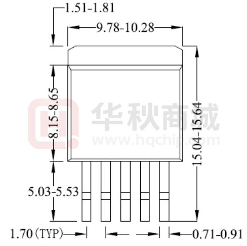
TO263-5 Package Outline Drawing
Bottom View
Sil
erg
yC
orp
.C
on
fi
de
nti
a
lP
Top View
Side View
Notes:
Recommended PCB Layout
(Reference only)
All dimension in millimeter and exclude mold flash & metal burr.
AN_SY6103 Rev0.9A
© 2021 Silergy Corp.
Silergy Corp. Confidential- Prepared for Customer Use Only
11
All Rights Reserved.
�SY6103
rep
are
dF
or
W
OO
KO
O
TO252-5 Package Outline & PCB Layout
Side View
Sil
erg
yC
orp
.C
on
fi
de
nti
a
lP
Top View
Bottom View
PCB layout (Recommended)
Notes: 1,All dimension in MM and exclude mold flash & metal burr
2,Recommended PCB layout only for reference.
AN_SY6103 Rev0.9A
© 2021 Silergy Corp.
Silergy Corp. Confidential- Prepared for Customer Use Only
12
All Rights Reserved.
�SY6103
Taping & Reel Specification
1. Taping Orientation for Packages
rep
are
Feeding direction
dF
or
W
OO
KO
O
TO252-5, TO263-5
TO252-5
on
fi
Pocket
pitch(mm)
Reel size
(Inch)
Trailer
length(mm)
Leader length
(mm)
Qty per
reel(pcs)
12
8
13"
400
400
800
8
13"
400
400
2500
erg
TO263-5
Tape width
(mm)
Sil
Package
type
yC
orp
.C
Reel
Size
de
nti
a
lP
2. Carrier Tape & Reel specification for packages
12
3. Others: NA
AN_SY6103 Rev0.9A
© 2021 Silergy Corp.
Silergy Corp. Confidential- Prepared for Customer Use Only
13
All Rights Reserved.
�SY6103
Revision History
The revision history provided is for informational purpose only and is believed to be accurate, however, not
warranted. Please make sure that you have the latest revision.
Revision
Change
Jun.17, 2021
Revision 0.9A
Update the package outline for TO252-5 (page12).
Dec.27, 2017
Revision 0.9
Initial Release
Sil
erg
yC
orp
.C
on
fi
de
nti
a
lP
rep
are
dF
or
W
OO
KO
O
Date
AN_SY6103 Rev0.9A
© 2021 Silergy Corp.
Silergy Corp. Confidential- Prepared for Customer Use Only
14
All Rights Reserved.
�SY6103
IMPORTANT NOTICE
1. Right to make changes. Silergy and its subsidiaries (hereafter Silergy) reserve the right to change any information
published in this document, including but not limited to circuitry, specification and/or product design, manufacturing or
descriptions, at any time and without notice. This document supersedes and replaces all information supplied prior to the
publication hereof. Buyers should obtain the latest relevant information before placing orders and should verify that such
information is current and complete. All semiconductor products are sold subject to Silergy’s standard terms and conditions of
sale.
dF
or
W
OO
KO
O
2. Applications. Application examples that are described herein for any of these products are for illustrative purposes only.
Silergy makes no representation or warranty that such applications will be suitable for the specified use without further testing or
modification. Buyers are responsible for the design and operation of their applications and products using Silergy products.
Silergy or its subsidiaries assume no liability for any application assistance or designs of customer products. It is customer’s sole
responsibility to determine whether the Silergy product is suitable and fit for the customer’s applications and products planned.
To minimize the risks associated with customer’s products and applications, customer should provide adequate design and
operating safeguards. Customer represents and agrees that it has all the necessary expertise to create and implement safeguards
which anticipate dangerous consequences of failures, monitor failures and their consequences, lessen the likelihood of failures
that might cause harm and take appropriate remedial actions. Silergy assumes no liability related to any default, damage, costs or
problem in the customer’s applications or products, or the application or use by customer’s third-party buyers. Customer will
fully indemnify Silergy, its subsidiaries, and their representatives against any damages arising out of the use of any Silergy
components in safety-critical applications. It is also buyers’ sole responsibility to warrant and guarantee that any intellectual
property rights of a third party are not infringed upon when integrating Silergy products into any application. Silergy assumes no
responsibility for any said applications or for any use of any circuitry other than circuitry entirely embodied in a Silergy product.
lP
rep
are
3. Limited warranty and liability. Information furnished by Silergy in this document is believed to be accurate and reliable.
However, Silergy makes no representation or warranty, expressed or implied, as to the accuracy or completeness of such
information and shall have no liability for the consequences of use of such information. In no event shall Silergy be liable for
any indirect, incidental, punitive, special or consequential damages, including but not limited to lost profits, lost savings, business
interruption, costs related to the removal or replacement of any products or rework charges, whether or not such damages are
based on tort or negligence, warranty, breach of contract or any other legal theory. Notwithstanding any damages that customer
might incur for any reason whatsoever, Silergy’ aggregate and cumulative liability towards customer for the products described
herein shall be limited in accordance with the Standard Terms and Conditions of Sale of Silergy.
on
fi
de
nti
a
4. Suitability for use. Customer acknowledges and agrees that it is solely responsible for compliance with all legal, regulatory
and safety-related requirements concerning its products, and any use of Silergy components in its applications, notwithstanding
any applications-related information or support that may be provided by Silergy. Silergy products are not designed, authorized or
warranted to be suitable for use in life support, life-critical or safety-critical systems or equipment, nor in applications where
failure or malfunction of an Silergy product can reasonably be expected to result in personal injury, death or severe property or
environmental damage. Silergy assumes no liability for inclusion and/or use of Silergy products in such equipment or
applications and therefore such inclusion and/or use is at the customer’s own risk.
orp
.C
5. Terms and conditions of commercial sale. Silergy products are sold subject to the standard terms and conditions of
commercial sale, as published at http://www.silergy.com/stdterms, unless otherwise agreed in a valid written individual
agreement specifically agreed to in writing by an authorized officer of Silergy. In case an individual agreement is concluded only
the terms and conditions of the respective agreement shall apply. Silergy hereby expressly objects to and denies the application
of any customer’s general terms and conditions with regard to the purchase of Silergy products by the customer.
Sil
erg
yC
6. No offer to sell or license. Nothing in this document may be interpreted or construed as an offer to sell products that is
open for acceptance or the grant, conveyance or implication of any license under any copyrights, patents or other industrial or
intellectual property rights. Silergy makes no representation or warranty that any license, either express or implied, is granted
under any patent right, copyright, mask work right, or other intellectual property right. Information published by Silergy
regarding third-party products or services does not constitute a license to use such products or services or a warranty or
endorsement thereof. Use of such information may require a license from a third party under the patents or other intellectual
property of the third party, or a license from Silergy under the patents or other intellectual property of Silergy.
For more information, please visit: www.silergy.com
© 2021 Silergy Corp.
AN_SY6103 Rev0.9A
© 2021 Silergy Corp.
Powered by TCPDF (www.tcpdf.org)
All Rights Reserved.
Silergy Corp. Confidential- Prepared for Customer Use Only
15
All Rights Reserved.
�