Application Note: SY6703
Low Voltage H-Bridge IC
Preliminary Specification
AN_SY6703 Rev.0.2
Silergy Corp. Confidential-prepared for Customer Use Only
1
�AN_SY6703
Pinout (top view)
nSLEEP
1
16
AIN1
AOUT1
2
15
AIN2
AISEN
3
14
VINT
AOUT2
4
13
GND
BOUT2
5
12
VM
BISEN
6
11
VCP
BOUT1
7
10
BIN2
nFAULT
8
9
BIN1
Package type
SY6703HFC
TSSOP-16E
①
Top Mark
AZRxyz
r
Part Number
Number
nSLEEP
1
AOUT1
2
AISEN
3
AOUT2
BOUT2
4
5
BISEN
6
BOUT1
nFAULT
BIN1
BIN2
VCP
VM
GND
VINT
AIN2
AIN1
GND
7
8
9
10
11
12
13
14
15
16
17
Description
Sleep mode pin. Logic low puts device in low-power sleep mode, this pin has a internal pull-down
resistor
Bridge A output 1 pin. Connect this pin to motor winding.
Bridge A current sense pin. Connect a resistor between this pin and GND for current control, or
connect to GND is current control is not needed.
Bridge A output 2 pin. Connect this pin to motor winding.
Bridge B output 2 pin. Connect this pin to motor winding.
Bridge B current sense pin. Connect a resistor between this pin and GND for current control, or
connect to GND is current control is not needed
Bridge B output 1 pin. Connect this pin to motor winding.
Fault state output pin. Logic low if fault is detected.
Bridge B input 1 pin. Control the state of bridge B, this pin has a internal pull-down resistor.
Bridge B input 2 pin. Control the state of bridge B, this pin has a internal pull-down resistor
Internal charge pump voltage for high side gate driver. Connect a ceramic capacitor to VM.
Motor power supply pin. Decouple this pin to GND pin with 0.1uF ceramic cap.
Device ground pin.
Internal logic and driver supply. Connect this pin with a ceramic capacitor to GND.
Bridge A input 2 pin. Control the state of bridge A, this pin has a internal pull-down resistor.
Bridge A input 1 pin. Control the state of bridge A, this pin has a internal pull-down resistor.
Ground pin for thermal dissipation.
Sil
er
gy
Co
rp
.C
on
fid
en
tia
l-P
re
p
Name
ar
ed
Note① : x=year code, y=week code, z= lot number code.
fo
17
GND
AN_SY6703 Rev.0.2
Silergy Corp. Confidential-prepared for Customer Use Only
2
�AN_SY6703
AN_SY6703 Rev.0.2
Silergy Corp. Confidential-prepared for Customer Use Only
3
�AN_SY6703
Electrical Characteristics
(TA = 25°C, VM=5V, unless otherwise specified)
Parameter
Power Supplies
VM Operating Supply Current
VM Sleep Mode Current
VM Undervoltage Lockout Voltage
Symbol
Test Conditions
IVM
IVMS
VUVLO_RISE
VUVLO_FALL
nSLEEP=0V, VM=5V
VM Rising
VM Falling
Min
VM=5V, xIN=0V, xIN2=0V
Typ
Max
Unit
1
1.8
2.2
2.1
2
2.5
mA
0.5
0.7
V
µA
V
V
Logic Level Input
VIL
nSLEEP
All other pins
nSLEEP
All other pins
VIH
VIHYS
IIL
IIH
Input High Current
RPD
Pulldown Resistance
IO=5mA
VO=3.3V
High Side MOSFETs On Resistance
Rdson
Low Side MOSFETs On Resistance
er
gy
Sil
Startup Time
ns
0.5
1
V
µA
310
400
410
mΩ
310
270
330
±1
2
150
VTRIP
tBLANK
kΩ
260
Internal PWM Frequency
VM=5V,16Ω to GND, 10% to
90% VM
VM=5V
VM=5V
IOCP
tOCPR
tDEG
TSD
THYS
tWAKE
6.6
16.5
600
150
450
V
µA
µA
1
13
33
330
fid
.C
on
fPWM
tR
tF
tPROP
tDEAD
VM=5V, IO=500mA, TJ=25℃
VM=5V, IO=500mA, TJ=85℃
VM=2.7V, IO=500mA, TJ=25℃
VM=2.7V, IO=500mA, TJ=85℃
VM=5V, IO=500mA, TJ=25℃
VM=5V, IO=500mA, TJ=85℃
VM=2.7V, IO=500mA, TJ=25℃
VM=2.7V, IO=500mA, TJ=85℃
VM=5V, VOUT=0V, TJ=25℃
en
IOFF
Co
rp
Off-State Leakage Current
Motor Driver
Current Control PWM Frequency
Rise Time
Fall Time
Propagation Delay INx to OUTx
Dead Time
Protection
Output Over Current Limit
Over Current Retry Time
OCP Deglitch Time
Thermal Shutdown Temperature
Thermal Shutdown hysteresis
Current Control
xISEN Trip Voltage
Current Sense Blanking Time
Sleep Mode
0.4
VIN=0V
VIN=3.3V, nSLEEP
VIN=3.3V, all except nSLEEP
nSLEEP
All other pins
r
Input Deglitch Time
tDEG
nFAULT Output (Open-Drain Output)
Output Low Voltage
VOL
Output High Leakage Current
IOH
H-Bridge MOSFETs
V
fo
Input Hysteresis
Input Low Current
2.5
2
ar
ed
Input High Voltage
tia
l-P
re
p
Input Low Voltage
160
µA
50
50
50
1.1
50
kHz
ns
ns
µs
ns
2.5
1.2
180
160
20
A
ms
ns
℃
℃
200
3.75
180
240
mV
µs
1
ms
nSLEEP Inactive high to Hbridge On
Note 1: Stresses beyond the “Absolute Maximum Ratings” may cause permanent damage to the device. These are
stress ratings only. Functional operation of the device at these or any other conditions beyond those indicated in the
operational sections of the specification is not implied. Exposure to absolute maximum rating conditions for
extended periods may affect device reliability.
Note 2: θ JA is measured in the natural convection at TA = 25°C on a low effective single layer thermal conductivity
test board of JEDEC 51-3 thermal measurement standard.
Note 3: Power dissipation and thermal limits must be observed.
AN_SY6703 Rev.0.2
Silergy Corp. Confidential-prepared for Customer Use Only
4
�AN_SY6703
AN_SY6703 Rev.0.2
Silergy Corp. Confidential-prepared for Customer Use Only
5
�AN_SY6703
AN_SY6703 Rev.0.2
Silergy Corp. Confidential-prepared for Customer Use Only
6
�AN_SY6703
Functional Description
PWM Motor Drivers
tia
l-P
re
p
ar
ed
fo
r
SY6703 contains two identical H-bridge motor drivers with current-control PWM circuitry. A block diagram of
the circuitry is shown below:
H-Bridge Driving Control
fid
en
Figure3. Motor Control Circuitry
xIN2
0
1
0
1
er
gy
Co
rp
xIN1
0
0
1
1
.C
on
The Bridge is controlled by a PWM input interface, also called IN/IN interface. The following table shows the
control logic of the device:
Table 1 H-Bridge Logic
xOUT1
Z
L
H
L
xOUT2
Z
H
L
L
Function
Coast/Fast Decay
Reverse
Forward
Brake/Slow Decay
Sil
The inputs can also be used for PWM control of the motor speed. When controlling a winding with PWM, when the
drive current is interrupted, the inductive nature of the motor requires that the current must continue to flow. This is
called recirculation current. To handle this recirculation current, the H-bridge can operate in two different states, fast
decay or slow decay. In fast decay mode, the H-bridge is disabled and recirculation current flows through the body
diodes; in slow decay, the motor winding is shorted.
To PWM using fast decay, the PWM signal is applied to one xIN pin while the other is held low; to use slow decay,
one xIN pin is held high.
AN_SY6703 Rev.0.2
Silergy Corp. Confidential-prepared for Customer Use Only
7
�AN_SY6703
Table 2 PWM Control of Motor Speed
xIN1
PWM
1
0
PWM
xIN2
0
PWM
PWM
1
Function
Forward PWM, Fast Decay
Forward PWM, Slow Decay
Reverse PWM, Fast Decay
Reverse PWM, Slow Decay
Figure 4 shows the current paths in different drive and decay modes.
Forward
Reverse
Figure4. Decay Mode
Current Control
The current through the motor windings may be limited, or controlled, by a fixed-frequency PWM current regulation,
or current chopping. For DC motors, current control is used to limit the start-up and stall current of the motor. For
stepper motors, current control is often used at all times.
When an H-bridge is enabled, current rises through the winding at a rate dependent on the DC voltage and
inductance of the winding. If the current reaches the current chopping threshold, the bridge disables the current until
the beginning of the next PWM cycle. Note that immediately after the current is enabled, the voltage on the xISEN
pin is ignored for a fixed period of time before en
AN_SY6703 Rev.0.2
Silergy Corp. Confidential-prepared for Customer Use Only
8
�AN_SY6703
If a 1-Ω sense resistor is used, the chopping current will be 200 mV/1 Ω = 200 mA.
Once the chopping current threshold is reached, the H-bridge switches to slow decay mode. Winding current is recirculated by enabling both of the low-side FETs in the bridge. This state is held until the beginning of the next
fixed-frequency PWM cycle.
Note that if current control is not needed, the xISEN pins should be connected directly to ground.
Sleep Mode
ar
ed
fo
r
Driving nSLEEP low will put the device into a low power sleep state. In this state, the H-bridges are disabled, the
gate drive charge pump is stopped, all internal logic is reset, and all internal clocks are stopped. All inputs are
ignored until nSLEEP returns inactive high. When returning from sleep mode, some time (up to 1 ms) needs to pass
before the motor driver becomes fully operational. To make the board design simple, the nSLEEP can be pulled up
to the supply (VM). It is recommended to use a pullup resistor when this is done. This resistor limits the current to
the input in case VM is higher than 6.5 V. Internally, the nSLEEP pin has a 500-kΩ resistor to GND. It also has a
clamping zener diode that clamps the voltage at the pin at 6.5 V. Currents greater than 250 µA can cause damage to
the input structure. Hence the recommended pullup resistor would be between 20 kΩ and 75 kΩ.
Protection Circuits
tia
l-P
re
p
The device is fully protected against undervoltage, overcurrent, and overtemperature.
Overcurrent Protection (OCP)
fid
en
An analog current limit circuit on each FET limits the current through the FET by limiting the gate drive. If this
analog current limit persists for longer than the OCP deglitch time, all FETs in the H-bridge will be disabled and the
nFAULT pin will be driven low. The driver will be re-enabled after the OCP retry period (tOCP) has passed.
nFAULT becomes high again at this time. If the fault condition is still present, the cycle repeats. If the fault is no
longer present, normal operation resumes and nFAULT remains deasserted. Please note that only the H-bridge in
which the OCP is detected will be disabled while the other bridge will function normally.
.C
on
Overcurrent conditions are detected independently on both high and low side devices; i.e., a short to ground, supply,
or across the motor winding will all result in an overcurrent shutdown. Note that overcurrent protection does not use
the current sense circuitry used for PWM current control, so functions even without presence of the xISEN resistors.
Co
rp
Thermal Shutdown (TSD)
If the die temperature exceeds safe limits, all MOSFETs in the H-bridge are disabled. Once the die temperature has
fallen to a safe level, operation automatically resumes.
er
gy
Undervoltage Lockout(UVLO)
Sil
If at any time the voltage on the VM pin falls below the undervoltage lockout threshold voltage, all circuitry in the
device will be disabled, and all internal logic will be reset. Operation will resume when VM rises above the UVLO
threshold. nFAULT is driven low in the event of an undervoltage condition.
THERMAL INFORMATION
Thermal Protection
The device has thermal shutdown (TSD) as described in the Protection Circuits section. If the die temperature
exceeds approximately 160°C, the device is disabled until the temperature drops to a safe level.
AN_SY6703 Rev.0.2
Silergy Corp. Confidential-prepared for Customer Use Only
9
�AN_SY6703
Any tendency of the device to enter thermal shutdown is an indication of either excessive power dissipation,
insufficient heatsinking, or too high an ambient temperature.
Maximum Output Current
In actual operation, the maximum output current achievable with a motor driver is a function of die temperature.
This in turn is greatly affected by ambient temperature and PCB design. Basically, the maximum motor current will
be the amount of current that results in a power dissipation level that, along with the thermal resistance of the
package and PCB, keeps the die at a low enough temperature to stay out of thermal shutdown.
The dissipation ratings given in the datasheet can be used as a guide to calculate the approximate maximum power
dissipation that can be expected to be possible without entering thermal shutdown for several different PCB
constructions. However, for accurate data, the actual PCB design must be analyzed via measurement or thermal
simulation.
Power Dissipation
2
(2)
ar
ed
PTOT = R DSON × I OUT ( RMS )
fo
r
Power dissipation in the device is dominated by the power dissipated in the output MOSFET resistance, or RDSON.
A H-bridge Average power dissipation can be roughly estimated by:
tia
l-P
re
p
where PTOT is the total power dissipation, RDSON is the resistance of the HS plus LS MOSFETs, and IOUT(RMS) is
the RMS or DC output current being supplied to the load.
The maximum amount of power that can be dissipated in the device is dependent on ambient temperature and
heatsinking.
Sil
er
gy
Co
rp
.C
on
fid
en
Note that RDSON increases with temperature, so as the device heats, the power dissipation increases.
AN_SY6703 Rev.0.2
Silergy Corp. Confidential-prepared for Customer Use Only
10
�AN_SY6703
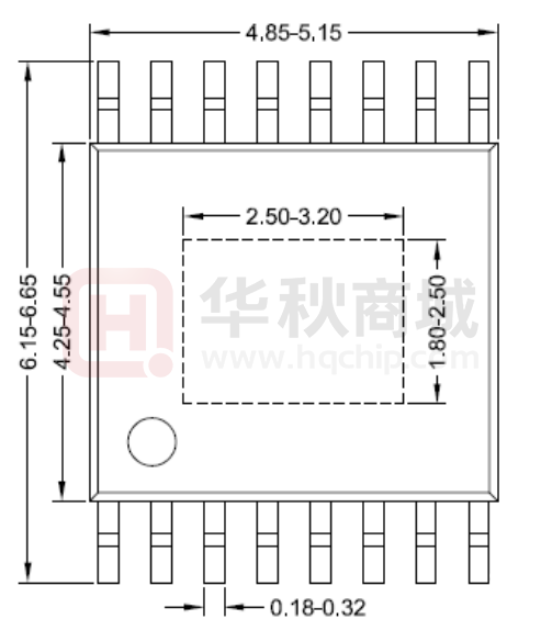
Side view A
Sil
er
gy
Co
rp
.C
on
Top view
fid
en
tia
l-P
re
p
ar
ed
fo
r
TSSOP16E Package Outline Drawing
Side view B
Notes:
All dimension in MM and exclude mold flash & metal burr.
AN_SY6703 Rev.0.2
Silergy Corp. Confidential-prepared for Customer Use Only
11
�