Application Note: SY67134
Medium Voltage H-Bridge IC
Features
The SY67134 operates with a power-supply voltage
range from 5V to 40V, and 3.6A maximum output
current. To be compatible with industry-standard
devices, the SY67134 uses the PWM input interface.
The SY67134 also provides over current protection,
under voltage lockout and thermal shutdown
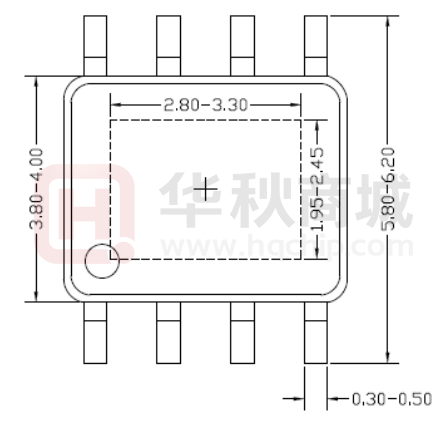
protection. The device is packaged in SO8E.
Temperature Code
Package Code
Optional Spec Code
de
nti
a
on
fi
.C
Typical Application
Note
erg
yC
orp
VM
Sil
lP
SY67134 □(□□)□
Package type
SO8E
Consumer Products
Robotics
rep
are
dF
Applications
Ordering Information
Ordering Number
SY67134FCC
Power Supply Voltage Range from 5V to 40V
3.6A Maximum Drive Current
H-bridge Motor Driver
PWM Interface
Low Power Standby Mode with Less than 15µA
Supply Current
Internal Over Current Protection, Under Voltage
Lockout and Thermal Shutdown
Automatic Fault Recovery
Synchronous Rectification
Compact Package: SO8E
OO
KO
O
The SY67134 is a H-bridge motor driver solution for
motion-control applications. The highly integrated Hbridge driver block consists of two half-bridges with
internal logic control, gate drive, over current
protection and charge pump circuit.
or
W
General Description
VM
OUT1
GND
DC
Motor
IN1
IN2
VREF
OUT2
ISEN
RSENSE
Figure1. Typical Application Circuit
AN_SY67134 Rev.0.9
© 2019 Silergy Corp.
Silergy Corp. Confidential-prepared for Customer Use Only
1
All Rights Reserved.
�AN_SY67134
Pin out (Top View)
SY67134
GND
1
8 OUT2
IN2
2
IN1
3
6 OUT1
VREF
4
5
VM
(SO8E)
OO
KO
O
7 ISEN
Thermal
Pad
VREF
4
VM
5
OUT1
ISEN
OUT2
Thermal
Pad
6
7
8
Description
Ground pin.
Logic input 2 pin. Logic high set OUT2 High, this pin has an internal pull-down resistor.
Logic input 1 pin. Logic high set OUT1 High, this pin has an internal pull-down resistor.
Current regulator voltage reference. ICHOP=VREF/10/RSENSE. Decouple this pin to GND
with at least 0.1uF ceramic capacitor.
Power supply pin. Decouple this pin to GND with 10uF ceramic cap and sufficient
electronic capacitor.
Output 1 pin. Connect this pin to motor winding.
Current sense resistor connection pin.
Output 2 pin. Connect this pin to motor winding.
Exposed pad for enhanced thermal dissipation. Connect to ground for maximum thermal
efficiency.
dF
Number
1
2
3
-
de
nti
a
lP
rep
are
Name
GND
IN2
IN1
or
W
Top Mark: CFXxyz (device code: CFX, x=year code, y=week code, z= lot number code)
.C
on
fi
Block Diagram
Power
management
Charge
pump
OUT1
Control
logic
Gate
Drive&OCP
erg
IN1
yC
orp
VM
IN2
Sil
OUT2
GND
+ -
Temperature
Sensor
ISEN
VREF
Figure2. Block Diagram
AN_SY67134 Rev.0.9
© 2019 Silergy Corp.
Silergy Corp. Confidential-prepared for Customer Use Only
2
All Rights Reserved.
�AN_SY67134
Absolute Maximum Ratings (Note 1)
OO
KO
O
VM, OUT1, OUT2 -------------------------------------------------------------------------------------------------- -0.3V to 40V
IN1, IN2 ---------------------------------------------------------------------------------------------------------------- -0.3V to 6V
VREF ------------------------------------------------------------------------------------------------------------------- -0.3V to 4V
ISEN--------------------------------------------------------------------------------------------------------------------- -0.3V to 4V
Junction Temperature (TJ) -------------------------------------------------------------------------------------- -40°C to +150°C
Storage Temperature ---------------------------------------------------------------------------------------- -55°C to +150°C
Package Thermal Resistance
θ JA (Note 2) ---------------------------------------------------------------------------------------------------- 62°C/W
θ JC (Note 2) ---------------------------------------------------------------------------------------------------- 20°C/W
Recommended Operating Conditions
Sil
erg
yC
orp
.C
on
fi
de
nti
a
lP
rep
are
dF
or
W
VM, OUT1, OUT2 ----------------------------------------------------------------------------------------------------- 5V to 32V
IN1, IN2 ------------------------------------------------------------------------------------------------------------------- 0V to 5V
VREF -------------------------------------------------------------------------------------------------------------------- 0V to 3.3V
ISEN------------------------------------------------------------------------------------------------------------------ -0.3V to 0.3V
RSENSE---------------------------------------------------------------------------------------------------------------less than 100mΩ
Logic Input PWM Frequency ---------------------------------------------------------------------------------- 0Hz to 100 kHz
H-Bridge Output Current (Note3) ------------------------------------------------------------------------------------- 0 to 3.6A
Junction Temperature Range ------------------------------------------------------------------------------------ -40°C to 125°C
Ambient Temperature Range ------------------------------------------------------------------------------------ -40°C to 85°C
AN_SY67134 Rev.0.9
© 2019 Silergy Corp.
Silergy Corp. Confidential-prepared for Customer Use Only
3
All Rights Reserved.
�AN_SY67134
Electrical Characteristics
Min.
Typ.
dF
rep
are
32
5
V
V
mV
µA
mA
OO
KO
O
4.7
200
1.5
-1
20
0
50
0.1
9.5
1
12
lP
de
nti
a
Unit
2
24
15
3
0.5
1
100
V
V
µA
µA
500
mΩ
±500
500
nA
ns
3
V
10.5
3
35
V/V
µs
µs
1
3.65
4.5
1.5
3
ms
5.5
A
µs
ms
165
°C
30
°C
.C
on
fi
Max.
5
or
W
(TA = 25°C, VM=24V, unless otherwise specified)
Parameter
Symbol
Test Conditions
Power Supply
Supply Voltage Range
VM
Under Voltage Threshold
VUVLO_TH
VM Rising
Under Voltage Hysteresis
VUVLO_HYS
Low power standby mode
VM Operating Supply
IIN
Current
很抱歉,暂时无法提供与“SY67134FCC”相匹配的价格&库存,您可以联系我们找货
免费人工找货- 国内价格
- 1+4.00820
- 10+3.24380
- 30+2.86160
- 100+2.48920