H75XX-2
200mA Current、35V Input Voltage LDO
H75XX-2
General Description
The H75XX-2 series is a set of three-terminal low
power high voltage regulators implemented in CMOS
technology. They allow input voltages as high as 35V.
They are available with several fixed output voltages
ranging from 3.0V to 5.0V. CMOS technology
ensures low voltage drop and low quiescent current.
Although designed primarily as fixed voltage
regulators, these devices can be used with external
components to obtain variable voltages and currents.
Features
●
●
●
●
●
●
Low power consumption
Low temperature coefficient
Low voltage drop
High input voltage (up to 35V)
Output voltage accuracy: tolerance ±2%
TO92, SOT89 and SOT23-3 package
Applications
● Battery-powered equipment
● Communication equipment
● Audio/Video equipment
Shanghai Siproin Microelectronics Co.
V2.0
1
�H75XX-2
Order specification
Part No
Package
Manner of Packing
Devices per bag/reel
H75XX-2TX
TO92
Bag
1000PCS/bag
H75XX-2PX
SOT89
Reel
1000PCS/reel
H75XX-2MX
SOT23-3
Reel
3000PCS/reel
Description of selection
Part No
Output Voltage
Output Voltage Accuracy
H7530-2XX
3.0V
±2%
H7533-2XX
3.3V
±2%
H7536-2XX
3.6V
±2%
H7544-2XX
4.4V
±2%
H7550-2XX
5.0V
±2%
Print rules
Package
Marking
TO92
75XX-H#
SOT89
75XX-H#
SOT23-3
XX-H
Note:”XX” stands for output voltages. Other voltages can be specially customized.
TO92 & SOT89 packages will add a “#” mark at the end of the marking.
Type selection guide
H75①②③④⑤
Designator
Symbol
①②
Integer
③
-2
Standard
T
Package:TO-92
P
Package:SOT89
M
Package:SOT23-3
R
RoHS / Pb Free
G
Halogen Free
④
⑤
Shanghai Siproin Microelectronics Co.
Description
Output Voltage(3.0~5.0V)
V2.0
2
�H75XX-2
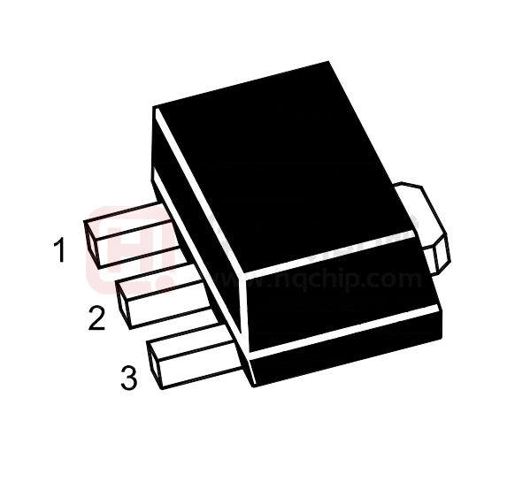
Block Diagram and Pin Arrangement Diagram
Pin Assignment
Pin No.
Pin Name
1
GND
Ground connection.
2
VIN
Supply Voltage Input.
3
VOUT
Shanghai Siproin Microelectronics Co.
Description
Output.
V2.0
3
�H75XX-2
Functional Description
The H75XX-2 series is a set of three-terminal low power high voltage regulators
implemented in CMOS technology. They allow input voltages as high as 35V. They
are available with several fixed output voltages ranging from 3.0V to 5.0V.
Absolute Maximum Ratings
Parameter
Symbol
Value
Unit
Supply Voltage Input
VIN
-0.3~35
V
Operating Temperature
Tamb
-40~85
℃
Storage Temperature
Tstg
-50~125
℃
Note: These are stress ratings only. Stresses exceeding the range specified under “Absolute
Maximum Ratings” may cause substantial damage to the device. Functional operation of
this device at other conditions beyond those listed in the specification is not implied and
prolonged exposure to extreme conditions may affect device reliability.
Thermal Information
Parameter
Thermal Resistance (Junction to
Ambient) (Assume no ambient
airflow, no heat sink)
Power Dissipation
Symbol
θ JA
PD
Package
Max.
Unit
SOT23-3
500
℃/W
SOT89
200
℃/W
TO92
200
℃/W
SOT23-3
0.20
W
SOT89
0.50
W
TO92
0.50
W
Note: P D is measured at Ta= 25℃
Shanghai Siproin Microelectronics Co.
V2.0
4
�H75XX-2
Electrical Characteristics
H7530-2,+3.0V Output Type
Parameter
Symbol
Test Conditions
V IN
Conditions
Min.
Typ.
Max.
Unit
Output
Voltage
V OUT
8V
I OUT =10mA
2.940
3.000
3.060
V
Output
Current
I OUT
6V
-
-
200
-
mA
Load
Regulation
ΔV OUT
8V
1mA≤I OUT ≤
20mA
-
40
60
mV
Voltage
Drop(Note)
V DIF
-
-
10
-
mV
ISS
8V
No load
-
2.0
5.0
μA
VOUT
VIN VOUT
-
4V≤V IN ≤35V
I OUT =1mA
-
0.3
-
%/V
Input Voltage
V IN
-
-
-
-
35
V
Temperature
Coefficient
VOUT
Ta
8V
-
±0.12
-
mV/℃
Current
Consumption
Line
Regulation
I OUT =1mA
ΔV OUT =2%
I OUT =10mA
0℃
很抱歉,暂时无法提供与“H7533-2PR”相匹配的价格&库存,您可以联系我们找货
免费人工找货- 国内价格
- 5+0.89975
- 50+0.71313
- 150+0.61982
- 1000+0.52650
- 2000+0.47056
- 5000+0.44248


 工商网监
湘ICP备2023018690号
工商网监
湘ICP备2023018690号
