TX78LXX
http://www.txsemi.com
Features
Output Current of 150mA
Output transistor safe area protection
Thermal Overload Protection
No external components
Short Circuit Protection
Package:SOT89-3 ,SOT23 and TO92
Output voltage accuracy: tolerance ±5%
General Description
TX78LXX is three-terminal positive regulators.
replacement for a zener diode-resistor
One of these regulators can deliver up to 150 mA
Combination, an effective improvement in output
of output current. The internal limiting and thermal
impedance can be obtained, together with lower
-shutdown features of the regulator make them
quiescent current.
essentially immune to overload. When used as a
Selection Table
Part No.
TX78L33
TX78L05
TX78L06
TX78L08
TX78L09
TX78L12
TX78L15
TX78L18
TX78L24
Ver2.4
Output Voltage
3.3V
5.0V
6.0V
8.0V
9.0V
12V
15V
18V
24V
Package
SOT23
SOT89
TO92
1
Marking
78L33
78L05
78L06
78L08
78L09
78L12
78L15
78L18
78L24
Jun.13,2022
�TX78LXX
http://www.txsemi.com
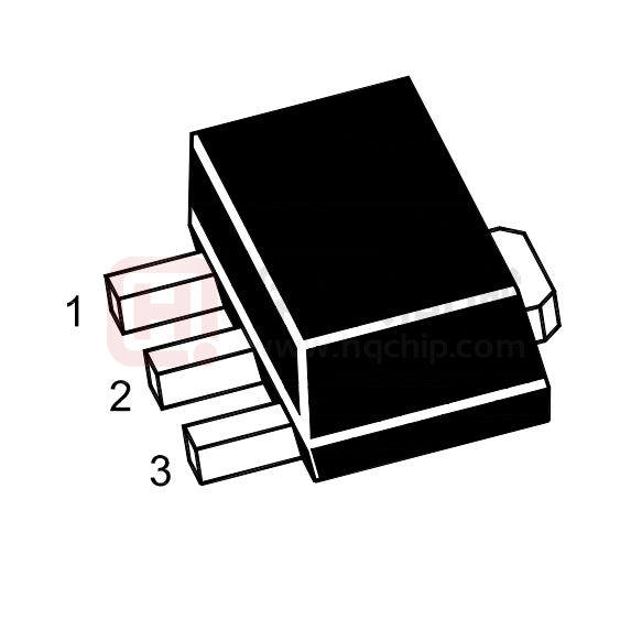
Pin Configuration
SOT89 (Top View)
Table1: TX78LXX series (SOT89 PKG)
PIN NO.
PIN NAME
FUNCTION
1
VOUT
Output voltage pin
2
GND
GND pin
3
VIN
Input voltage pin
SOT23 (Top View)
Table2: TX78LXX series (SOT23 PKG)
PIN NO.
PIN NAME
FUNCTION
1
VOUT
Output voltage pin
2
VIN
Input voltage pin
3
GND
GND pin
TO92 (Top View)
Table3: TX78LXX series (TO92 PKG)
Ver2.4
PIN NO.
PIN NAME
FUNCTION
1
VOUT
Output voltage pin
2
GND
GND pin
3
VIN
Input voltage pin
2
Jun.13,2022
�TX78LXX
http://www.txsemi.com
Block Diagram
Absolute Maximum Ratings(Ta=25℃)
Parameter
Rating
Unit
Input supply voltage: VIN MAX
30
V
MAX. Output current: Iout
150
mA
MAX Power:
SOT89
0.5
W
Pmax
SOT23
0.2
W
Junction temperature: Tj
-55~150
℃
Operation temperature: Topr
-40~125
℃
Storage temperature: Tstr
-55~155
℃
Soldering temperature and time
+260(Recommended 10S)
℃
ESD Rating, (HBM)
2
KV
Note: The absolute maximum ratings are rated values exceeding which the product could suffer physical
damage. These values must therefore not be exceeded under any conditions.
Ver2.4
3
Jun.13,2022
�TX78LXX
http://www.txsemi.com
Electrical Characteristics
(Cin=0.33uF, Co=0.1uF, Ta=25℃,unless otherwise noted)
Parameter
Symbol
Conditions
Min.
Typ.
Max.
Io=40mA, VIN=10V
0.964vout
vout
1.036vout
0.96vout
vout
1.04vout
0.95vout
vout
1.05vout
VIN=7V~18V, Io=20mA
-150
-
150
VIN=8V~18V, Io=20mA
-100
-
100
-100
-
100
Io=1mA~40mA
Output Voltage
Vout
VIN=7V~18V
Io=1mA~10mA
VIN=10V
Line Regulation
LNR
VIN=10V,
Load Regulation
LDR
Io=1mA~100mA
VIN=10V,
Io=1mA~40mA
Dropout Voltage
Output noise
Voltage
mV
-30
-
30
-
2
-
V
VN
F=10Hz to 100KHz
-
40
-
uV/Vo
-
80
-
dB
VIN=10V, IOUT=40mA
-
-
5.5
mA
VIN=8V~18V, IO=20mA
-1.5
-
1.5
-0.1
-
0.1
Quiescent Current
IQ
Ta=25℃,f=120Hz,
Io=40mA, VIN=8V~20V
△IQ
VIN=10V,
IOUT=1mA~40mA,
LNR: Line Regulation. The change in output voltage for a change in the input voltage. The measurement
is made under conditions of low dissipation or by using pulse techniques such that the average chip
temperature is not significantly affected.
LDR: Load Regulation. The change in output voltage for a change in load current at constant chip
temperature.
Ver2.4
mV
Ta=25℃,Io=100mA
PSRR
Change
V
VDIF
Ripple Rejection
Quiescent Current
Unit
4
Jun.13,2022
mA
�TX78LXX
http://www.txsemi.com
Typical Performance Characteristics
Ver2.4
5
Jun.13,2022
�TX78LXX
http://www.txsemi.com
Operation Description
TX78LXX is designed with Thermal Overload Protection that shuts down the circuit when subjected to an
excessive power overload condition, and Output Transistor Safe-Area Compensation that reduces the
output short circuit current as the voltage across the pass transistor is increased.
In many low current applications, compensation capacitors are not required. However, it is recommended
that the regulator input be bypassed with a capacitor if the regulator is connected to the power supply
filter with long wire lengths, or if the output load capacitance is large. An input bypass capacitor should be
selected to provide good high frequency characteristics to insure stable operation under all load
conditions. A 0.33μFor larger tantalum, mylar, or other capacitor having low internal impedance at high
frequencies should be chosen. The bypass capacitor should be mounted with the shortest possible leads
directly across the regulator’s input terminals. Normally good construction techniques should be used to
minimize ground loops and lead resistance drops since the regulator has no external sense lead.
Typical Application
Fig.1 Typical Application
A common ground is required between the input and the output voltages. The input voltage must remain
typically 2.0 V above the output voltage even during the low point on the input ripple voltage.
Cin is required if regulator is located an appreciable distance from power supply filter.
Co is not needed for stability; however, it does improve transient response.
Fig.2 Constant Current Regulator
Ver2.4
6
Jun.13,2022
�TX78LXX
http://www.txsemi.com
Package Information
3-pin SOT89 Outline Dimensions
Ver2.4
7
Jun.13,2022
�TX78LXX
http://www.txsemi.com
3-pin SOT23 Outline Dimensions
Ver2.4
8
Jun.13,2022
�TX78LXX
http://www.txsemi.com
3-pin TO92 Outline Dimensions
Ver2.4
9
Jun.13,2022
�TX78LXX
http://www.txsemi.com
© Shanghai TX Electronics Sci-Tech Co., Ltd
TX cannot assume responsibility for use of any circuitry other than circuitry entirely embodied in a TX
product. No circuit patent license, copyrights or other intellectual property rights are implied. TX reserves
the right to make changes to their products or specifications without notice. Customers are advised to
obtain the latest version of relevant information to verify, before placing orders, that information being
relied on is current and complete.
Ver2.4
10
Jun.13,2022
�
很抱歉,暂时无法提供与“TX78L05”相匹配的价格&库存,您可以联系我们找货
免费人工找货