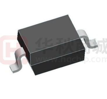
PTVSLC3D8VB
Low Capacitance TVS
Description
The PTVSLC3D8VB is a low capacitance transient voltage suppressor for
high speed data interface that designed to protect sensitive electronics
from damage or latch-up due to ESD lightning, and other voltage induced
transient events.
All pins are rated to withstand 15kV ESD pulses using the IEC61000-4-2
air discharge method, which can meet the requirement of level 4.
Applications
Feature
350W peak pulse power per line (tP = 8/20μs)
Ethernet – 10/100/1000 Base T
SOD-323 package
Cellular phones
Replacement for MLV(0805)
Handheld-wireless systems
Bidirectional configurations
PDAs
Protects one power or I/O port
USB interface
Low clamping voltage
RoHS compliant
Transient protection for data lines to IEC61000-4-2(ESD)
±30kV(air), ±30kV(contact); IEC61000-4-4 (EFT) 80A (5/50ns)
Mechanical Characteristics
Lead finish:100% matte Sn(Tin)
Mounting position: Any
Qualified max reflow temperature:260℃
Pure tin plating: 7 ~ 17 um
Pin flatness:≤3mil
Electronics Parameter
Symbol
VRWM
IR
VBR
Rev.06.2
Parameter
Peak Reverse Working Voltage
IPP
Reverse Leakage Current @ VRWM
I
Breakdown Voltage @ IT
IT
Test Current
IPP
Maximum Reverse Peak Pulse Current
VC
Clamping Voltage @ IPP
PPP
Peak Pulse Power
CJ
Junction Capacitance
IF
Forward Current
VF
Forward Voltage @ IF
VC VBR VRWM
IT
IR
V
IR
IT
VRWM VBR VC
IPP
1
www.prisemi.com
�Low Capacitance TVS
PTVSLC3D8VB
Electrical characteristics per line@25℃( unless otherwise specified)
Parameter
Symbol
Peak Reverse Working Voltage
Conditions
Min.
Typ.
VRWM
Breakdown Voltage
Max.
Units
8
V
VBR
It = 1mA
Reverse Leakage Current
IR
VRWM = 8V T=25℃
1.0
μA
Clamping Voltage
VC
IPP = 1A tP = 8/20μs
13.0
V
Clamping Voltage
VC
IPP=18A tP = 8/20μs
31.6
V
Junction Capacitance
Cj
VR=0V
8.5
f = 1MHz
V
4.5
pF
Absolute maximum rating@25℃
Rating
Symbol
Value
Units
Peak Pulse Power (tp=8/20μs)
Ppp
350
W
Operating Temperature
TJ
-55 to +150
℃
TSTG
-55 to +150
℃
Storage Temperature
Typical Characteristics
100
% Of Rated Power
IPP – Peak Pulse Current - % of
IPP
tf=8μs
100
80
60
tP =20μs(IPP /2)
40
20
0
80
60
40
20
0
5
10
15
t - Time -μs
20
25
0
30
Fig 1.Pulse Waveform
Rev.06.2
0
25
50
75
100
125
TL – Lead Temperature - ℃
150
Fig 2.Power Derating Curve
2
www.prisemi.com
�Low Capacitance TVS
PTVSLC3D8VB
10000
40
Pulse waveform: tp=8/20us
1000
Peak Pulse Power (W)
VC-Clamping Voltage (V)
32
24
16
100
8
10
0
5
10
15
20
IPP-Peak pulse current(A)
25
30
Fig 3. Clamping voltage vs. Peak pulse current
1
10
100
Pulse Duration(us)
1000
Fig 4. Non Repetitive Peak Pulse Power vs. Pulse time
Solder Reflow Recommendation
Peak Temp=257℃, Ramp Rate=0.802deg. ℃/sec
280
240
200
160
120
80
40
0
0
30
60
90
120
150
180
240
210
270
300
330
360
390
420
450
480
Time (sec)
PCB Design
For TVS diodes a low-ohmic and low-inductive path to chassis earth is absolutely mandatory in order to achieve good ESD
protection. Novices in the area of ESD protection should take following suggestions to heart:
Do not use stubs, but place the cathode of the TVS diode directly on the signal trace.
Do not make false economies and save copper for the ground connection.
Place via holes to ground as close as possible to the anode of the TVS diode.
Use as many via holes as possible for the ground connection.
Keep the length of via holes in mind! The longer the more inductance they will have.
Rev.06.2
3
www.prisemi.com
�Low Capacitance TVS
PTVSLC3D8VB
Product dimension (SOD-323)
C
Dim
A
E
B
F
D
H
Inches
Millimeters
MIN
MAX
MIN
MAX
A
0.063
0.075
1.60
1.90
B
0.045
0.057
1.15
1.45
C
0.090
0.106
2.30
2.70
D
0.031
0.043
0.80
1.00
E
0.010
0.01
0.25
0.40
F
0.004
0.007
0.09
0.18
H
0.000
0.004
0.00
0.10
3.00
0.90
0.80
Suggested
PCB Layout
Unit:mm
Marking information
HC
Ordering information
Device
Package
Reel
Shipping
PTVSLC3D8VB
SOD-323 (Pb-Free)
7"
3000 / Tape & Reel
Rev.06.2
4
www.prisemi.com
�Low Capacitance TVS
PTVSLC3D8VB
IMPORTANT NOTICE
and
are registered trademarks of Prisemi Electronics Co., Ltd (Prisemi) ,Prisemi
reserves the right to make changes without further notice to any products herein. Prisemi makes
no warranty, representation or guarantee regarding the suitability of its products for any particular
purpose, nor does Prisemi
assume any liability arising out of the application or use of any
product or circuit, and specifically disclaims any and all liability, including without limitation
special, consequential or incidental damages. “Typical” parameters which may be provided in
Prisemi data sheets and/or specifications can and do vary in different applications and actual
performance may vary over time. All operating parameters, including “Typicals” must be
validated for each customer application by customer’s technical experts. Prisemi does not
convey any license under its patent rights nor the rights of others. The products listed in this
document are designed to be used with ordinary electronic equipment or devices, Should you
intend to use these products with equipment or devices which require an extremely high level of
reliability and the malfunction of with would directly endanger human life (such as medical
instruments, aerospace machinery, nuclear-reactor controllers, fuel controllers and other safety
devices), please be sure to consult with our sales representative in advance.
Website: http://www.prisemi.com
For additional information, please contact your local Sales Representative.
©Copyright 2009, Prisemi Electronics
is a registered trademark of Prisemi Electronics.
All rights are reserved.
Rev.06.2
5
www.prisemi.com
�
很抱歉,暂时无法提供与“PTVSLC3D8VB”相匹配的价格&库存,您可以联系我们找货
免费人工找货- 国内价格
- 5+0.33151
- 20+0.30226
- 100+0.27301
- 500+0.24375
- 1000+0.23010
- 2000+0.22035
