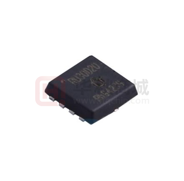
PE507BA
P-Channel Logic Level Enhancement Mode
Field Effect Transistor
NIKO-SEM
PDFN 3x3P
Halogen-free & Lead-Free
D
PRODUCT SUMMARY
V(BR)DSS
RDS(ON)
ID
-30V
14mΩ
-42A
D
D D D
G
#1 S
S
G : GATE
D : DRAIN
S : SOURCE
S S G
ABSOLUTE MAXIMUM RATINGS (T A = 25 °C Unless Otherwise Noted)
PARAMETERS/TEST CONDITIONS
SYMBOL
LIMITS
UNITS
Drain-Source Voltage
VDS
-30
V
Gate-Source Voltage
VGS
±25
V
Continuous Drain Current
3
TC = 25 °C
-42
TC = 100 °C
-26
ID
TA = 25 °C
-12
TA = 70 °C
Pulsed Drain Current
1
IDM
-80
IAS
-42
EAS
87
Avalanche Current
Avalanche Energy
Power Dissipation
L = 0.1mH
4
A
-9.7
TC = 25 °C
37
TC = 100 °C
15
PD
TA = 25 °C
mJ
W
3.1
TA = 70 °C
2
Junction & Storage Temperature Range
Tj, Tstg
-55 to 150
°C
THERMAL RESISTANCE RATINGS
THERMAL RESISTANCE
SYMBOL
TYPICAL
MAXIMUM
Junction-to-Ambient
2
t ≦10s
RθJA
40
Junction-to-Ambient
2
Steady-State
RθJA
60
RJC
3.3
Junction-to-Case
UNITS
°C / W
1
Pulse width limited by maximum junction temperature.
2
The value of RθJA is measured with the device mounted on 1in FR-4 board with 2oz. Copper, in a still air
environment with TA =25°C.
3
Package limitation current is 22A
4
The Power dissipation is based on RJA t ≦10s value.
2
REV1.2
K-11-3
1
�PE507BA
P-Channel Logic Level Enhancement Mode
Field Effect Transistor
NIKO-SEM
PDFN 3x3P
Halogen-free & Lead-Free
ELECTRICAL CHARACTERISTICS (TJ = 25 °C, Unless Otherwise Noted)
LIMITS
PARAMETER
SYMBOL
TEST CONDITIONS
MIN
UNIT
TYP MAX
STATIC
Drain-Source Breakdown Voltage
V(BR)DSS
VGS = 0V, ID = -250A
-30
VGS(th)
VDS = VGS, ID = -250A
-1
Gate-Body Leakage
IGSS
VDS = 0V, VGS = ±25V
±100
VDS = -24V, VGS = 0V
-1
Zero Gate Voltage Drain Current
IDSS
VDS = -20V, VGS = 0V, TJ = 55 °C
-10
Gate Threshold Voltage
Drain-Source On-State Resistance
Forward Transconductance
1
1
V
-1.5
-3
VGS = -4.5V, ID = -9A
14.5
22
RDS(ON)
VGS = -10V, ID = -10A
9.6
14
gfs
VDS = -10V, ID = -10A
32
nA
A
mΩ
S
DYNAMIC
Input Capacitance
Ciss
Output Capacitance
Coss
Reverse Transfer Capacitance
Crss
Gate Resistance
Rg
Total Gate Charge
2
2
2
Turn-Off Delay Time
Fall Time
2
2
Turn-On Delay Time
Rise Time
VGS = 0V, VDS = -15V, f = 1MHz
2
2
365
pF
327
VGS = 0V, VDS = 0V, f = 1MHz
Qg
Gate-Source Charge
Gate-Drain Charge
2100
Ω
3
49.1
VDS = -15V , VGS = -10V,
ID = -10A
Qgs
6
Qgd
12.3
td(on)
24
tr
VDD = -15V
24
td(off)
ID -10A, VGS = -10V, RGEN = 6Ω
85
tf
nC
nS
50
SOURCE-DRAIN DIODE RATINGS AND CHARACTERISTICS (T J = 25 °C)
Continuous Current
Forward Voltage
1
IS
VSD
Reverse Recovery Time
trr
Reverse Recovery Charge
Qrr
IF = -10A, VGS = 0V
IF=-10A, dI/dt=100A/μs
-30
A
-1.2
V
20.5
nS
8.3
uC
Pulse test : Pulse Width 300 sec, Duty Cycle 2%.
Independent of operating temperature.
1
2
REV1.2
K-11-3
2
�P-Channel Logic Level Enhancement Mode
Field Effect Transistor
NIKO-SEM
PDFN 3x3P
Halogen-free & Lead-Free
Output Characteristics
Transfer Characteristics
50
VGS=-10V
VGS=-7V
VGS=-5V
VGS=-4.5V
VGS=-4V
40
-ID, Drain-To-Source Current(A)
-ID, Drain-To-Source Current(A)
50
30
VGS=-3V
20
10
VGS=-2.5V
0
40
30
20
25℃
10
125℃
-20℃
0
0
1
2
3
4
5
0
1
-VDS, Drain-To-Source Voltage(V)
3
4
5
Capacitance Characteristic
2500
VDS=-15V
ID=-10A
8
C , Capacitance(pF)
-VGS , Gate-To-Source Voltage(V)
2
-VGS, Gate-To-Source Voltage(V)
Gate charge Characteristics
Characteristics
10
6
4
2
2000
CISS
1500
1000
500
COSS
CRSS
0
0
0
10
20
30
40
50
0
6
Qg , Total Gate Charge(nC)
0.03
12
18
24
30
-VDS, Drain-To-Source Voltage(V)
On-Resistance VS Drain Current
On-Resistance VS Gate-To-Source
Voltage
0.02
0.025
RDS(ON)ON-Resistance(OHM)
RDS(ON)ON-Resistance(OHM)
PE507BA
0.02
0.015
0.01
0.005
ID=-10A
0
0.015
VGS=-4.5V
0.01
VGS=-10V
0.005
0
3
4
5
6
7
8
9
10
0
-VGS, Gate-To-Source Voltage(V)
10
20
30
40
50
-ID , Drain-To-Source Current(A)
REV1.2
K-11-3
3
�PDFN 3x3P
Halogen-free & Lead-Free
On-Resistance VS Temperature
Source-Drain Diode Forward Voltage
100
1.4
-IS , Source Current(A)
Normalized Drain to Source
ON-Resistance
1.5
1.3
1.2
1.1
1.0
0.9
125℃
25℃
10
1
VGS=-10V
ID=-10A
0.8
0.7
0.1
-50
-25
0
25
50
75
100
125
150
0.0
0.2
0.4
TJ , Junction Temperature(˚C)
0.6
0.8
1.0
1.2
1.4
-VSD, Source-To-Drain Voltage(V)
Safe Operating Area
Single Pulse Maximum Power Dissipation
100
120
10
Power(W)
-ID , Drain Current(A)
PE507BA
P-Channel Logic Level Enhancement Mode
Field Effect Transistor
NIKO-SEM
1ms
10ms
1
Operation in This
Area is Limited by
RDS(ON)
0.1
90
60
100ms
1S
10S
NOTE :
1.VGS= 10V
2.TA=25˚C
3.RθJA = 60˚C/W
4.Single Pulse
30
DC
0
0.001
0.01
0.1
Single Pulse
RθJA = 60˚C/W
TA=25˚C
1
10
100
0.01
0.1
-VDS, Drain-To-Source Voltage(V)
1
10
100
Single Pulse Time(s)
Transient Thermal Response Curve
Transient Thermal Resistance
r(t) , Normalized Effective
10
1
Duty cycle=0.5
0.2
0.1
0.1
0.05
Notes
0.02
0.01
0.01
0.001
0.0001
single pulse
0.001
1.Duty cycle, D= t1 / t2
2.RthJA = 60 ℃/W
3.TJ-TA = P*RthJA(t)
4.RthJA(t) = r(t)*RthJA
0.01
0.1
1
10
100
1000
T1 , Square Wave Pulse Duration[sec]
REV1.2
K-11-3
4
�
很抱歉,暂时无法提供与“PE507BA”相匹配的价格&库存,您可以联系我们找货
免费人工找货- 国内价格
- 1+1.82747
- 10+1.43554
- 30+1.26760
- 100+1.05808
- 500+0.96477
- 1000+0.82426
