SHENZHEN CLOUDCHILD TECHNOLOGY CO., LTD
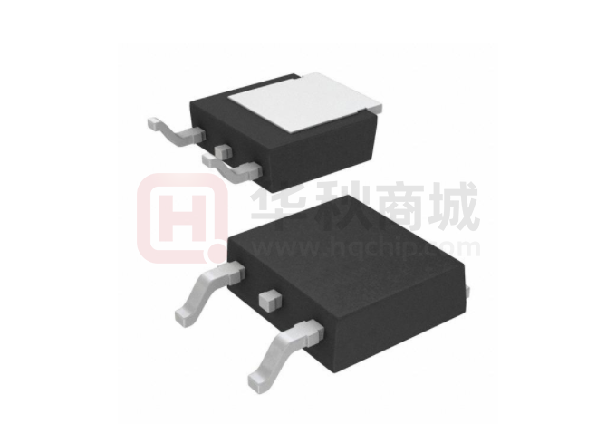
TO-252 Silicon N-Channel Power MOSFET
CCMC03N120 N-Channel
MOSFET
VDSS
RDS(ON)(Typ.)
ID
1200V
6.7Ω
3A
Applications:
●
●
●
Adaptor
Electric welder
SMPS
Features:
●
RoHS Compliant
●
Low ON Resistance
●
Low Gate Charge
●
Peak Current vs Pulse Width Curve
●
Inductive Switching Curves
●
AEC Q101 Qualified
Ordering Information
PART NUMBER
CCMC03N120
PACKAGE
TO-252
Absolute Maximum Ratings
Symbol
VDSS
ID
IDM
PD
VGS
EAS
dv/dt
Tj=25℃unless otherwise specified
Parameter
Rating
Drain-to-Source Voltage
Units
1200
V
3
1.8
A
A
12
A
Power Dissipation TC =25℃
83
W
Derating Factor above 25℃
Gate-to-Source Voltage
0.8
±30
W/℃
V
Single Pulse Avalanche Energy(NOTE *2)
30
mJ
Peak Diode Recovery dv/dt(NOTE *3)
5
V/ns
Continuous Drain Current TC =25℃
Continuous Drain Current TC =100℃
Pulsed Drain Current (NOTE *1)
Operating Junction and Storage
TJ and TSTG
℃
175,-55 to175
Temperature Range
Thermal Resistance
Symbol
Parameter
Max.
Units
℃∕W
RθJC
Junction-to-Case
1.5
RθJA
Junction-to-Ambient
120
www.cloudchild.cn
Test Conditions
Water cooled heatsink, PD adjusted for a
peak junction temperature of +150℃.
1 cubic foot chamber, free air.
Rev. - 1.0
�MOSFET ELECTRICAL CHARACTERISTICS
OFF Characteristics
Symbol
BVDSS
IDSS
Tj=25℃unless otherwise specified
Parameter
Drain-to-Source Breakdown Voltage
Min.
Typ.
Max.
Units
Test Conditions
1200
--
--
V
VGS=0V, ID=250μA
--
--
25
VDS=1200V, VGS=0V
μA
Drain-to-Source Leakage Current
--
--
TJ=25℃
VDS=960V, VGS=0V
250
TJ=125℃
IGSS
Gate-to-Source Forward Leakage
--
--
+100
Gate-to-Source Reverse Leakage
--
--
-100
ON Characteristics
Symbol
nA
VGS=+30V
VGS= -30V
TJ=25℃unless otherwise specified
Parameter
Min.
Typ.
Max.
Units
Test Conditions
RDS(ON)
StaticDrain-to-Source On-Resistance
--
6.7
9
Ω
VGS=10V, ID=1.5A
VGS(TH)
Gate Threshold Voltage
3
--
5
V
VDS=VGS,ID=250μA
gfs
Forward Transconductance
--
5
--
S
VDS=15V, ID=1.5A
Pulse width ≤300μs; duty cycle≤ 2%
Dynamic Characteristics
Symbol
Essentially independent of operating temperature
Parameter
Min.
Typ.
Max. Units
Rg
Gate resistance
--
2.2
--
Ciss
Coss
Input Capacitance
--
1006
--
Output Capacitance
--
59.8
--
Crss
Qg
Reverse Transfer Capacitance
--
2.2
--
Total Gate Charge
--
19.7
--
Qgs
Gate-to-Source Charge
--
7.5
--
Qgd
Gate-to-Drain (“Miller”) Charge
--
5.4
--
Resistive Switching Characteristics
Symbol
Parameter
td(ON)
Turn-on Delay Time
trise
Rise Time
td(OFF)
Turn-Off Delay Time
tfall
Fall Time
www.cloudchild.cn
Test Conditions
Ω
f = 1.0MHz
pF
VGS= 0V,VDS = 25V
f =1.0MHz
nC
ID=3A,VDD=960V
VGS = 10V
Essentially independent of operating temperature
Min.
Typ.
Max. Units
Test Conditions
-15.1
-VDD=600V, ID=3A,
-19.4
-ns
VG=10V RG=10Ω
-25.6
---
76.2
--
Rev. - 1.0
�Source-Drain Diode Characteristics
Symbol
IS
ISM
Parameter
Continuous Source Current
(Body Diode)
Maximum Pulsed Current
(Body Diode)
Tj=25℃unless otherwise specified
Min.
Typ.
Max.
Units
--
--
3
A
Test Conditions
TC=25℃
--
--
12
A
VSD
Diode Forward Voltage
--
--
1.5
V
trr
Reverse Recovery Time
--
526
--
ns
IF= IS
nC
di/dt=100A/us
Qrr
Reverse Recovery Charge
--
2000
--
ISD=3A, VGS=0V
Pulse width ≤300μs; duty cycle ≤ 2%
Notes:
*1. Repetitive rating; pulse width limited by maximum junction temperature.
*2. L=10mH, ID=2.5A, Start TJ=25℃
*3. ISD =3A,di/dt ≤100A/us,VDD≤BVDS, Start TJ=25℃
*4. Recommend soldering temperature defined by IPC/JEDEC J-STD 020
www.cloudchild.cn
Rev. - 1.0
�Characteristics Curve:
Figure 1 Maximum Continuous Drain Current vs
Figure 2 Typical Output Characteristics
Case Temperature
Figure 3 Typical Transfer Characteristics
www.cloudchild.cn
Figure 4 Typical Body Diode Transfer Characteristics
Rev. - 1.0
�Figure 5 Typical Drain to Source ON
Resistance vs Drain Current
Figure 7 Typical Theshold Voltage vs
Figure 6 Typical Drian to Source on Resistance
vs Junction Temperature
Figure 8 Typical Breakdown Voltage vs Junction
Junction TemperatureTemperature
www.cloudchild.cn
Rev. - 1.0
�Figure 9 Typical Capacitance vs Drain to
Source Voltage
www.cloudchild.cn
Figure 10 Typical Gate Charge vs Gate to
Source Voltage
Rev. - 1.0
�TO-252 Package Outline Dimensions
NOTICE
CLOUDCHILD reserves the right to make modifications,enhancements,improvements,corrections or
other changes without further notice to any product herein. CLOUDCHILD does not assume any
liability arising out of the application or use of any product described herein.
www.cloudchild.cn
Rev. - 1.0
�
很抱歉,暂时无法提供与“CCMC03N120”相匹配的价格&库存,您可以联系我们找货
免费人工找货- 国内价格
- 1+6.03787
- 30+5.82967
- 100+5.41326
- 500+4.99686
- 1000+4.78866