PED3312M
N-Channel Enhancement Mode Power MOSFET
Description
The PED3312M uses advanced trench technology to provide
excellent RDS(ON), low gate charge and operation with gate
voltages as low as 2.5V. This device is suitable for use as a
load switch or in PWM applications. It is ESD protected.
General Features
Schematic diagram
● VDS = 18V,ID =22 A
RDS(ON) < 4.5 mΩ @ VGS=4.5V
RDS(ON) < 4.7 mΩ @ VGS=3.8V
RDS(ON) < 6mΩ @ VGS=2.5V
ESD Rating: 2000V HBM
● High Power and current handing capability
● Lead free product is acquired
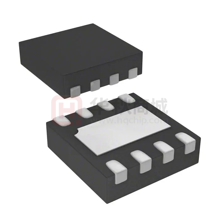
Marking and pin Assignment
● Surface Mount Package
Application
●PWM application
●Load switch
DFN3x3-8L top view
Absolute Maximum Ratings (TA=25℃unless otherwise noted)
LIMITS
Drain-Source Voltage
SYMBOL
VDS
Gate-Source Voltage
VGS
±10
PARAMETERS/TEST CONDITIONS
Continuous Drain Current
TA = 25 °C
ID
TA = 70 °C
Pulsed Drain Current (Note 1)
Avalanche Current
Avalanche Energy
Power Dissipation
L = 0.1mH
TA = 25 °C
www.semi-one.com
1
16
80
IAS
20
EAS
26
TJ, Tstg
Operating Junction & Storage Temperature Range
V
22
IDM
PD
TA = 70 °C
18
UNITS
3.6
2.4
-55 to 150
A
mJ
W
°C
2017. Feb. V1.0
�PED3312M
Thermal Characteristic
Thermal Resistance,Junction-to-Ambient (Note 2)
RθJA
℃/W
34.7
Notes:
1. Pulse width limited by maximum junction temperature.
2. The value of RJA is measured with the device mounted on 1in2 FR-4 board with 2oz. Copper, in a still air
environment with TA =25°C.
Electrical Characteristics (TA=25℃unless otherwise noted)
Parameter
Symbol
Condition
Min
Typ
Max
Unit
Off Characteristics
Drain-Source Breakdown Voltage
BVDSS
VGS=0V ID=250μA
18
20
-
V
Zero Gate Voltage Drain Current
IDSS
VDS=20V,VGS=0V
-
-
1
μA
Symbol
Condition
Min
Typ
Max
Unit
IGSS
VGS=±10V,VDS=0V
-
-
±10
μA
VGS(th)
VDS=VGS,ID=250μA
0.45
0.8
1.2
V
VGS=4.5V, ID= 8A
-
3.4
4.5
mΩ
VGS=3.8V, ID=7A
-
3.5
4.7
mΩ
VGS=2.5V, ID=6A
-
4.4
6
mΩ
VDS=5V,ID=5A
-
40
-
S
-
3140
-
PF
-
352
-
PF
-
PF
Parameter
Gate-Body Leakage Current
On Characteristics (Note 2)
Gate Threshold Voltage
Drain-Source On-State Resistance
Forward Transconductance
RDS(ON)
gFS
Dynamic Characteristics (Note 3)
Input Capacitance
Clss
Output Capacitance
Coss
Reverse Transfer Capacitance
Crss
-
320
Turn-on Delay Time
td(on)
-
20
nS
Turn-on Rise Time
tr
VDD=10V,RL=1.35Ω
-
40
nS
td(off)
VGS=5V,RGEN=3Ω
-
72
nS
-
16
nS
-
35
nC
-
3
-
nC
-
10
-
nC
-
-
1.2
V
-
-
26
A
VDS=10V,VGS=0V,
F=1.0MHz
Switching Characteristics (Note 3)
Turn-Off Delay Time
Turn-Off Fall Time
tf
Total Gate Charge
Qg
Gate-Source Charge
Qgs
Gate-Drain Charge
Qgd
VDS=10V,ID=7A,
VGS=4.5V
Drain-Source Diode Characteristics
Diode Forward Voltage (Note 2)
VSD
Diode Forward Current (Note 1)
IS
VGS=0V,IS=1A
Notes:
1. Surface Mounted on FR4 Board, t ≤ 10 sec.
2. Pulse Test: Pulse Width ≤ 300μs, Duty Cycle ≤ 2%.
3. Guaranteed by design, not subject to production
www.semi-one.com
2
2017. Feb. V1.0
�PED3312M
TYPICAL ELECTRICAL AND THERMAL CHARACTERISTICS
Vdd
Vgs
Rgen
td(on)
Rl
Vin
D
ton
tr
td(off)
90%
Vout
VOUT
G
toff
tf
90%
INVERTED
10%
10%
90%
S
VIN
50%
50%
10%
PULSE WIDTH
Figure 2:Switching Waveforms
PD Power(W)
Rdson On-Resistance(mΩ)
Figure 1:Switching Test Circuit
TJ-Junction Temperature(℃)
ID- Drain Current (A)
Figure 3 Power Dissipation
ID- Drain Current (A)
Normalized On-Resistance
Figure 4 Drain-Source On-Resistance
TJ-Junction Temperature(℃)
Vds Drain-Source Voltage (V)
Figure 5 Output CHARACTERISTICS
www.semi-one.com
Figure 6 Drain-Source On-Resistance
3
2017. Feb. V1.0
�C Capacitance (pF)
ID- Drain Current (A)
PED3312M
Vds Drain-Source Voltage (V)
Vgs Gate-Source Voltage (V)
Figure 8 Capacitance vs Vds
Rdson (mΩ)
Is- Reverse Drain Current (A)
Figure 7 Transfer Characteristics
Vgs Gate-Source Voltage (V)
Vds Drain-Source Voltage (V)
Figure 10 Capacitance vs Vds
Figure 9 Rdson vs Vgs
ID- Drain Current (A)
Vgs Gate-Source Voltage (V)
2
IDM =80A
ID=22A
10
7
5
3
2
1.0
7
5
3
2
DC
10
PW≤10μs
10
0μ
1m s
s
10
ms
0m
op
s
era
tio
Operation in this
area is limited by RDS(on).
0.1
7 Ta=25°C
5 Single pulse
3 When mounted on ceramic substrate
2
(900mm2✕0.8mm) 1unit
0.01
2 3 5 7 1.0
2 3
0.01 2 3 5 7 0.1
n
5 7 10
2 3
5
Vds Drain-Source Voltage (V)
Qg Gate Charge (nC)
Figure 11 Gate Charge
www.semi-one.com
100
7
5
3
2
Figure 12
4
Safe Operation Area
2017. Feb. V1.0
�r(t),Normalized Effective
Transient Thermal Impedance
PED3312M
Square Wave Pluse Duration(sec)
Figure 13 Normalized Maximum Transient Thermal Impedance
www.semi-one.com
5
2017. Feb. V1.0
�PED3312M
www.semi-one.com
6
2017. Feb. V1.0
�
很抱歉,暂时无法提供与“PED3312M”相匹配的价格&库存,您可以联系我们找货
免费人工找货