Application Note: SQ52110
Current Sensing Comparator with Overcurrent Protection
General Description
Features
The SQ52110 is a current sensing comparator with
overcurrent protection and used for the overcurrent
protection applications.
It measures the voltage across a shunt resistor and
compares this voltage with an adjustable threshold set
by an external resistor. Independent of the supply
voltage, SQ52110 can handle the common voltage
range between 0V and 36V and the differential input
range from 0mV to 250mV.
An open drain alert output can be configured to
operate in either a transparent mode where the output
status follows the input state or in a latched mode
where the alert output is cleared when the latch is
cleared. The device response time setting is
selectable, which enables overcurrent alerts to be
issued in as fast as 10μs.
The SQ52110 operates from a single 2.7V to 5.5V
supply, drawing a typical supply current of 135μA. It
is specified over the extended operating temperature
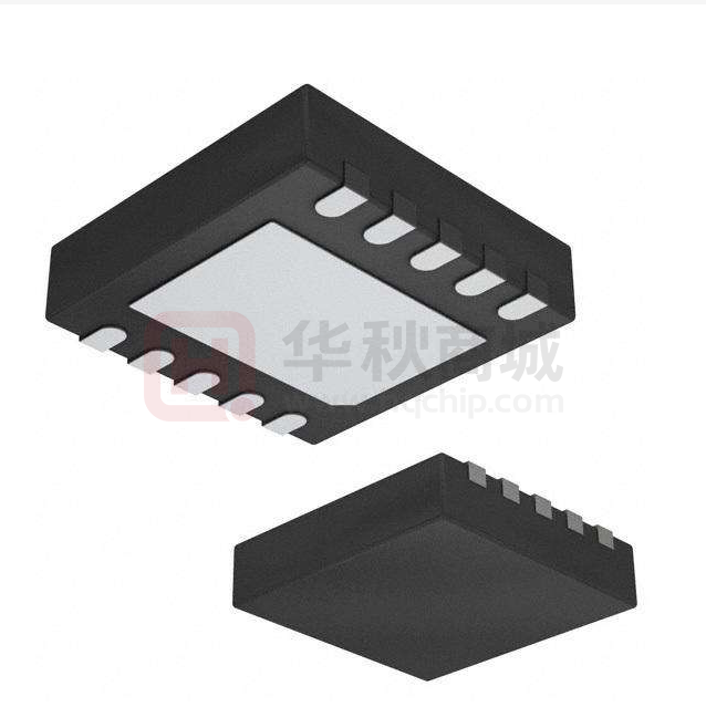
range of –40°C to +125°C, and is available in
DFN2×2-10 packages.
Ordering Information
SQ52110 □(□□□ )
Package Code
Wide Common Mode Range: 0V to 36V
Selectable Response Times: 10μs, 50μs, 100μs
Programmable Threshold:
Adjust Using Single Resistor
Programmable from 0 mV to 250 mV
Accuracy:
Offset Voltage: ±500μV (Max)
Offset Voltage Drift: 0.5μV/°C (Max)
Selectable Hysteresis: 2 mV, 4 mV, 8 mV
Active Quiescent Current: 135μA (Typ)
Selectable Disable Mode
Disabled Quiescent Current: 1.2μA (Max)
Disabled Input Bias Current: 500nA (Max)
Open Drain Output with Latch Mode Available
Applications
Overcurrent Protection
Computers
Servers
Telecom Equipment
Power Supplies
Battery Chargers
Optional Spec Code
Ordering Number
SQ52110TDD
Package type
Note
DFN2×2-10
Typical Application
2.7V to 5.5V
RPullup
VS
Power
Supply
0V to 36V
ENABLE
LATCH
IN+
Processor
GPIO
GPIO
+
CMP
IN-
ALERT
GPIO
LIMIT
DAC
DELAY
Load
RLIMIT
HYS
GND
Figure 1. Typical Application
AN_SQ52110 Rev. 0.9
© 2021 Silergy Corp.
Silergy Corp. Confidential- Prepared for Customer Use Only
1
All Rights Reserved.
�AN_SQ52110
Pin out
IN+
1
10
HYS
IN-
2
9
VS
LIMIT
3
8
GND
ENABLE
4
7
DELAY
ALERT
5
6
LATCH
Thermal
Pad
Top mark: W2xyz (Device code: W2, x=year code, y=week code, z= lot number code)
Pin Number
1
2
3
4
5
6
7
8
9
10
Thermal pad
Pin Name
IN+
INLIMIT
ENABLE
ALERT
LATCH
DELAY
GND
VS
HYS
Function Description
Connect to supply side of shunt resistor
Connect to load side of shunt resistor
Alert threshold limit input
Enable or disable selection input
Overlimit alert, active-low, open-drain output
Transparent or latch mode selection input
Response time selection input
Ground
Power supply, 2.7 V to 5.5 V
Hysteresis setting input
This pad can be connected to ground or left floating.
Absolute Maximum Ratings (Note 1)
VS---------------------------------------------------------------------------------------------------------------------------- -0.3V~6V
Differential VIN+ - VIN- -------------------------------------------------------------------------------------------------- -40V~40V
Common mode, VIN+, VIN- --------------------------------------------------------------------------------------------- -0.3V~40V
Alert output VALERT ------------------------------------------------------------------------------------------------------- -0.3V~6V
Input voltage at Any Pin------------------------------------------------------------------------------------------ -0.3V~VS+0.3V
Operating Temperature ------------------------------------------------------------------------------------------------- -40~125°C
Maximum Junction Temperature ------------------------------------------------------------------------------------------- 150°C
Storage Temperature Range --------------------------------------------------------------------------------------- -65°C ~ 150°C
ESD Susceptibility
HBM (Human Body Mode) -------------------------------------------------------------------------------------------------- ±2kV
CDM (Charged Device Mode) ----------------------------------------------------------------------------------------------- ±1kV
Recommended Operating Conditions
VS---------------------------------------------------------------------------------------------------------------------------------- 3.3V
Common mode, VIN+, VIN- ------------------------------------------------------------------------------------------------------ 12V
Delay setting ------------------------------------------------------------------------------------------------------------------- 100μs
Operating free-air Temperature---------------------------------------------------------------------------------------- -40~125°C
AN_SQ52110 Rev. 0.9
© 2021 Silergy Corp.
Silergy Corp. Confidential- Prepared for Customer Use Only
2
All Rights Reserved.
�AN_SQ52110
Electrical Characteristics
At TA=25°C, VIN=VIN+–VIN–=0mV, VS=3.3V, VIN+=12V, VLIMIT=10mV, and DELAY=100μs, unless otherwise
noted.
Symbol
Parameter
Conditions
Min
Typ
Max
Units
0
36
V
0
250
mV
Input
VCM
Common Mode Input Voltage
VIN
Differential Input Voltage
VIN=VIN+-VIN-
CMR
Common Mode Rejection
VIN=0V~36V, TA=-40°C~+125°C
VS=3.3V, DELAY=100μs
VS=3.3V, DELAY=50μs
VS=3.3V, DELAY=10μs
TA=-40°C~+125°C
VS=2.7V~5.5V, VIN+=12V,
TA=-40°C~+125°C
VOS
Offset Voltage, RTI
dVOS/dT
Offset Voltage Drift, RTI
PSR
Power Supply Rejection Ratio
IB
Input Bias Current(1)
IOS
Input Offset Current(2)
ILIMIT
Limit Threshold Output Current
110
Disable mode
TA=25°C
TA=-40°C~+125°C
19.85
19.8
120
-75
-125
-350
0.1
-500
-500
-650
0.5
dB
μV/°C
5
60
μV/V
3.5
0.05
±0.1
20
8
0.5
μA
μV
μA
20.15
20.2
μA
Digital Input/Output
tp
Alert Propagation Delay
HYS
Hysteresis
Delay=open, overdrive(3)=1mV
10
Delay=GND, overdrive=1mV
50
Delay=VS, overdrive=1mV
100
HYS=open
2
HYS=GND
4
HYS=VS
8
Latch, enable
μs
mV
1.4
6
VS-0.5
6
Latch, enable
0
0.4
Delay, hysteresis
0
0.5
VIH
High Level Input Voltage
VIL
Low Level Input Voltage
VOL
Alert Low Level Output Voltage
IOL=3mA
50
100
mV
ALERT Terminal Leakage Input
Current
VOH=3.3V
0.1
1
μA
1
2
μA
135
155
0.6
1.2
Digital Leakage Input Current
Delay, hysteresis
Pin ENABLE, LATCH, DELAY
and HYS, 0
很抱歉,暂时无法提供与“SQ52110TDD”相匹配的价格&库存,您可以联系我们找货
免费人工找货