TPL820 Series
42-V Input, 180-mA Output
High Voltage and Low Quiescent Current LDO
Features
Description
Wide Input Voltage Range: 3.6 V to 42 V
The TPL820 series products are high-performance
and low dropout linear regulators. The TPL820 series
products support a maximum 42 V input voltage and
180 mA output current with low quiescent current and
high PSRR. The TPL820 series products are stable
with a 2.2 μF to 22 μF output capacitor, and a 4.7 μF
ceramic capacitor is recommended.
Fixed Output: 2.8 V, 3 V, 3.3 V, and 5 V
±1% Output Accuracy Under Room Temperature
Ultra-Low Quiescent Current: 2 µA
Maximum Output Current: 180 mA
Low Dropout Voltage: 200 mV at 50 mA
High PSRR: 73 dB at 100 Hz
Current Limit and Thermal Protection
Stable with 2.2 μF to 22 μF Low ESR Ceramic
Capacitor
Soft Start Limits Input Current Surge During
Enable
Thermal Shutdown Protection
Junction Temperature Range: −40°C to +125°C
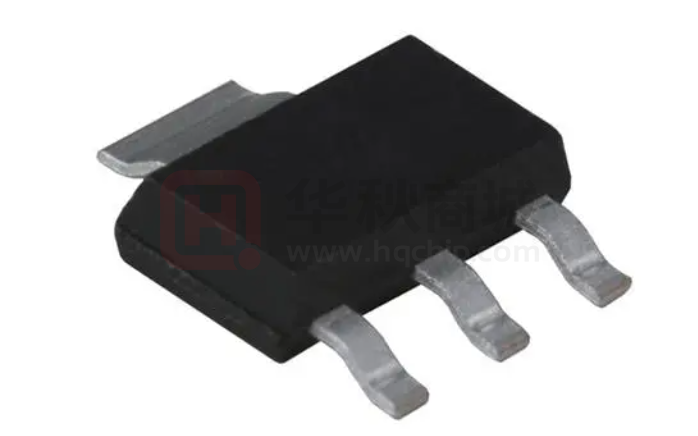
Packages: SOT89-3, SOT23-5, SOT23-3,
SOT223-3
Applications
Handheld Devices with Battery Power Supply
The TPL820 series products have a high PSRR with
73 dB at 100 Hz. This feature makes TPL820 series
products
very
suitable
for
power-sensitive
applications with high noise from the previous stage
power supply. 2 μA ultra-low quiescent current makes
the TPL820 series products ideal choices for portable
devices with battery power supply. Current-limit and
thermal overload protection circuits improve the
reliability under heavy load conditions.
The TPL820 series products provide fixed output
voltage options from 2.8 V to 5 V with ±2% voltage
accuracy over operating conditions. The TPL820
series products are guaranteed over the junction
temperature range from −40°C to +125°C.
POS and Power Tools
Meters and Smoke Detector
Industrial Control
Wireless and IoT Modules
Typical Application Schematic
Input
VOUT
VIN
CIN
TPL820
Output
COUT
GND
www.3peakic.com.cn
1 / 19
Rev.A.7
�TPL820 Series
42-V Input, 180-mA Output
High Voltage and Low Quiescent Current LDO
Product Family Table
Order Number
Output Voltage (V)
Package
TPL820F28-89TR
Fixed 2.8 V
SOT89-3
TPL820F30-89TR
Fixed 3.0 V
SOT89-3
TPL820F33-89TR
Fixed 3.3 V
SOT89-3
TPL820F50-89TR
Fixed 5.0 V
SOT89-3
TPL820F28-5TR
Fixed 2.8 V
SOT23-5
TPL820F30-5TR
Fixed 3.0 V
SOT23-5
TPL820F33-5TR
Fixed 3.3 V
SOT23-5
TPL820F50-5TR
Fixed 5.0 V
SOT23-5
TPL820U28-5TR
Fixed 2.8 V
SOT23-5 (B)
TPL820U30-5TR
Fixed 3.0 V
SOT23-5 (B)
TPL820U33-5TR
Fixed 3.3 V
SOT23-5 (B)
TPL820U50-5TR
Fixed 5.0 V
SOT23-5 (B)
TPL820F28-3TR
Fixed 2.8 V
SOT23-3
TPL820F30-3TR
Fixed 3.0 V
SOT23-3
TPL820F33-3TR
Fixed 3.3 V
SOT23-3
TPL820F50-3TR
Fixed 5.0 V
SOT23-3
TPL820F28-ST4R
Fixed 2.8 V
SOT223-3
TPL820F30-ST4R
Fixed 3.0 V
SOT223-3
TPL820F33-ST4R
Fixed 3.3 V
SOT223-3
TPL820F50-ST4R
Fixed 5.0 V
SOT223-3
www.3peakic.com.cn
2 / 19
Rev.A.7
�TPL820 Series
42-V Input, 180-mA Output
High Voltage and Low Quiescent Current LDO
Table of Contents
Features .............................................................................................................................................................. 1
Applications ....................................................................................................................................................... 1
Description ......................................................................................................................................................... 1
Typical Application Schematic ......................................................................................................................... 1
Product Family Table ......................................................................................................................................... 2
Revision History ................................................................................................................................................ 4
Pin Configuration and Functions ..................................................................................................................... 5
Pin Functions ................................................................................................................................................ 5
Specifications .................................................................................................................................................... 6
Absolute Maximum Ratings .......................................................................................................................... 6
ESD, Electrostatic Discharge Protection ...................................................................................................... 6
Recommended Operating Conditions .......................................................................................................... 6
Thermal Information ..................................................................................................................................... 6
Electrical Characteristics .............................................................................................................................. 7
Typical Performance Characteristics ............................................................................................................ 8
Detailed Description ........................................................................................................................................ 10
Overview..................................................................................................................................................... 10
Functional Block Diagram .......................................................................................................................... 10
Feature Description .................................................................................................................................... 10
Application and Implementation ..................................................................................................................... 11
Application Information ................................................................................................................................ 11
Typical Application ....................................................................................................................................... 11
Layout ............................................................................................................................................................... 12
Layout Guideline......................................................................................................................................... 12
Tape and Reel Information .............................................................................................................................. 13
Package Outline Dimensions ......................................................................................................................... 14
SOT89-3 ..................................................................................................................................................... 14
SOT23-5 ..................................................................................................................................................... 15
SOT23-3 ..................................................................................................................................................... 16
SOT223-3 ................................................................................................................................................... 17
Order Information ............................................................................................................................................ 18
www.3peakic.com.cn
3 / 19
Rev.A.7
�TPL820 Series
42-V Input, 180-mA Output
High Voltage and Low Quiescent Current LDO
Revision History
Date
Revision
2018-09-28
Rev.Pre
Preliminary version
2018-11-27
Rev.A.0
Initial release
2019-08-31
Rev.A.1
Added SOT223-3 package
2020-04-30
Rev.A.2
Updated thermal information of SOT89-3 package
2021-03-29
Rev.A.3
1. Changed the pin 1 orientation of the SOT23-3 package
2. Added Tape and Reel Information
2021-05-28
Rev.A.4
1. Corrected the Tape and Reel Information
2021-08-31
Rev.A.5
1. Changed output current from 200 mA to 180 mA
2022-03-21
Rev.A.6
1. Added output capacitor upper limit
2. Removed ambient temperature range
3. Removed 1.2 V, 1.8 V, 2.5 V, and 4.5 V output version
4. Removed SOT89-3 (B) package
2022-07-22
Rev.A.7
Corrected the typical application circuit in Figure 12
www.3peakic.com.cn
Notes
4 / 19
Rev.A.7
�TPL820 Series
42-V Input, 180-mA Output
High Voltage and Low Quiescent Current LDO
Pin Configuration and Functions
TPL820
TPL820
SOT89-3 Package
SOT23-5 Package
Top View
Top View
OUT
1
GND
2
IN
3
GND
IN
1
GND
2
NC
3
5
OUT
4
NC
TPL820
TPL820
SOT23-5 (B) Package
SOT23-3 Package
Top View
Top View
GND
1
IN
2
OUT
3
5
GND
NC
1
3
4
OUT
NC
IN
2
TPL820
3-Pin SOT223 Package
Top View
GND
1
OUT
2
IN
3
OUT
Pin Functions
Pin
SOT89
-3
SOT23
-5
SOT23
-5 (B)
SOT23
-3
SOT223
-3
Name
I/O
3
1
2
3
3
IN
I
Input voltage pin.
−
3, 4
4, 5
−
−
NC
−
No connection
1
5
3
2
2
OUT
O
Regulated output voltage pin.
2
2
1
1
1
−
Ground reference pin. Connect the GND
pin to PCB ground plane directly.
www.3peakic.com.cn
5 / 19
Description
Rev.A.7
�TPL820 Series
42-V Input, 180-mA Output
High Voltage and Low Quiescent Current LDO
Specifications
Absolute Maximum Ratings(1)
Parameter
Min
Max
Unit
VIN
Maximum Input Voltage
−0.3
45
V
VOUT
Maximum Output Voltage
−0.3
6
V
PD
Maximum Operating Power Dissipation
1.5
W
TJ
Junction Temperature Range
−40
150
°C
TSTG
Storage Temperature Range
−65
150
°C
TL
Lead Temperature (Soldering 10 sec)
260
°C
(1) Stresses beyond those listed under Absolute Maximum Ratings may cause permanent damage to the device. Exposure
to any Absolute Maximum Rating condition for extended periods may affect device reliability and lifetime.
(2) All voltage values are with respect to GND.
ESD, Electrostatic Discharge Protection
Symbol
Parameter
Condition
Minimum Level
Unit
±2.5
kV
±2
kV
JS-001(1)
HBM
Human Body Model ESD
ANSI/ESDA/JEDEC
CDM
Charged Device Model ESD
ANSI/ESDA/JEDEC JS-002(2)
(1) JEDEC document JEP155 states that 500-V HBM allows safe manufacturing with a standard ESD control process.
(2) JEDEC document JEP157 states that 250-V CDM allows safe manufacturing with a standard ESD control process.
Recommended Operating Conditions
Parameter
Min
Max
Unit
VIN
Input Voltage
3.6
42
V
VOUT
Output Voltage
1.2
5
V
IOUT
Output Current
0
180
mA
TJ
Operating Junction Temperature Range
−40
125
°C
Power Dissipation (SOT89-3 Package)
0
1000
mW
Power Dissipation (SOT23-5 Package)
0
300
mW
Power Dissipation (SOT23-3 Package)
0
300
mW
Power Dissipation (SOT223-3 Package)
0
PD
mW
Thermal Information
Package Type
θJA
θJC
Unit
SOT89-3
63.0
9.41
°C/W
SOT23-5
280
62
°C/W
SOT23-3
280
62
°C/W
SOT223-3
65
39
°C/W
www.3peakic.com.cn
6 / 19
Rev.A.7
�TPL820 Series
42-V Input, 180-mA Output
High Voltage and Low Quiescent Current LDO
Electrical Characteristics
All test conditions: VIN = VOUT(NOM) +1 V or 3.6 V, whichever is greater; COUT = 2.2 µF, TA = +25°C, unless
otherwise noted.
Symbol
Parameter
Conditions
Min
Typ
Max
Unit
42
V
5
µA
Supply Input Voltage and Current
VIN
Input Voltage Range
IQ
Quiescent Current
UVLO
VIN under-voltage Lock-out
3.6
IOUT = 0 mA
2
IOUT = 180 mA
390
µA
VIN rising
2.9
V
TJ = +25°C
1%
Regulated Output Voltage and Current
VOUT
ΔVOUT
Output Voltage Accuracy
–40°C ≤ TJ ≤ +125°C
2%
Line Regulation
VIN = VOUT(NOM) + 1 V to 42 V, or VIN ≥
3.6 V,IOUT = 1 mA
3
mV
Load Regulation
IOUT = 1 mA to 180 mA
20
mV
VIN = 0.98 × VOUT(NOM), IOUT = 50 mA
200
VIN = 0.98 × VOUT(NOM), IOUT = 180 mA
720
VDO (1)
Dropout Voltage
IOUT
Output Current
VOUT in regulation
ICL (2)
Output Current Limit
VOUT = 0.9 × VOUT(NOM)
PSRR
Power Supply Rejection
Ratio
VN
−2%
600
mV
mV
0
180
mA
180
800
mA
IOUT = 10 mA, f = 100 Hz, COUT = 4.7 µF
75
dB
IOUT = 10 mA, f = 1 kHz, COUT = 4.7 µF
65
dB
IOUT = 10 mA, f = 10 kHz, COUT = 4.7 µF
65
dB
IOUT = 10 mA, BW = 10 Hz to 100 kHz
110
μVRMS
IOUT = 10 mA, BW = 100 Hz to 100 kHz
70
μVRMS
Thermal Shutdown
Threshold
160
ºC
Hysteresis
40
ºC
Output Noise Voltage
Temperature Range
TSD
(1) Dropout voltage is the minimum input to output voltage differential needed to maintain regulation at a specified output
current. In dropout, the output voltage will be equal to V IN – VDO.
(2) Measured with VIN = VOUT +2.5 V.
www.3peakic.com.cn
7 / 19
Rev.A.7
�TPL820 Series
42-V Input, 180-mA Output
High Voltage and Low Quiescent Current LDO
Typical Performance Characteristics
All test conditions: VIN = VOUT(NOM) +1 V or 3.6 V, whichever is greater; COUT = 2.2 µF, TA = +25°C, unless
otherwise noted.
5
350
–40°C
300
25°C
250
85°C
Quiescent Current (µA)
Quiescent Current (µA)
400
200
150
100
50
4
3
2
–40°C
25°C
1
85°C
0
0
0
45
90
135
180
0
6
12
Load Current (mA)
Figure 1. Quiescent Current vs Output Current
30
36
42
1
–40°C
VIN = 12 V
4
Dropout Voltage (V)
QUiescent Current (µA)
24
Figure 2. Quiescent Current vs Input Voltage
5
3
2
1
0
0.8
25°C
85°C
0.6
0.4
0.2
0
-40
-15
10
35
60
85
0
45
Ambient Temperature (°C)
90
135
180
Load Current (mA)
Figure 3. Quiescent Current vs Ambient Temperature
Figure 4. Dropout Voltage vs Output Current
3.4
4.0
IOUT = 0 mA
3.35
Output Voltage (V)
Output Voltage (V)
18
Supply Voltage (V)
3.3
3.25
3.2
3.0
2.0
1.0
0.0
-40
-15
10
35
60
85
0
Ambient Temperature (°C)
12
18
24
30
36
42
Supply Voltage (V)
Figure 5. Output Accuracy vs Ambient Temperature
www.3peakic.com.cn
6
8 / 19
Figure 6. Output Voltage vs Input Voltage
Rev.A.7
�TPL820 Series
42-V Input, 180-mA Output
High Voltage and Low Quiescent Current LDO
Typical Performance Characteristics (Continued)
All test conditions: VIN = VOUT(NOM) + 1 V or 3.6 V, whichever is greater; COUT = 2.2 µF, TA = +25°C, unless
otherwise noted.
3.40
3.40
Output Voltage (V)
Output Voltage (V)
IOUT = 1 mA
3.35
3.30
–40°C
3.25
25°C
3.35
3.30
–40°C
3.25
25°C
85°C
85°C
3.20
3.20
0
6
12
18
24
30
36
42
0
45
Supply Voltage (V)
90
135
180
Load Current (mA)
Figure 7. Line Regulation
Figure 8. Load Regulation
4.0
90
70
3.0
PSRR (dB)
Output Voltage (V)
80
2.0
1.0
60
50
40
30
20
IOUT = 100 mA
10
0.0
0
0
200
400
10
Load Current (mA)
1K
10K
100K
1M
Frequency (Hz)
Figure 9. Current Limit
www.3peakic.com.cn
100
Figure 10. PSRR
9 / 19
Rev.A.7
�TPL820 Series
42-V Input, 180-mA Output
High Voltage and Low Quiescent Current LDO
Detailed Description
Overview
The TPL820 series products are 180-mA wide input range linear regulators with a very low quiescent current.
These voltage regulators operate from 3.6 V to 42 V and consume 2 μA of quiescent current at no load.
The TPL820 series products are available in fixed output voltage versions of 2.8 V, 3 V, 3.3 V, and 5 V with ±2%
output voltage accuracy over operating conditions.
Functional Block Diagram
IN
OUT
UVLO
Ban dgap
Regula tor
Control
+
–
VBG
Thermal
Shu tdo wn
GND
Curren t
Limit
Figure 11. TPL820 Series
Feature Description
Under-Voltage Lockout (UVLO)
The TPL820 series uses an under-voltage lock-out circuit (UVLO = 2.9 V) to keep the output shut off until the
internal circuitry operates properly.
Regulated Output Voltage
The TPL820 series products are available in fixed voltage versions of 2.8 V, 3 V, 3.3 V, and 5 V. When the input
voltage is higher than VOUT(NOM) + VDO or 3.6 V, the output pin is the regulated output based on the selected
voltage version. When the input voltage falls below V OUT(NOM) + VDO or 3.6 V, the output pin tracks the input
voltage minus the dropout voltage based on the load current. When the input voltage drops below the UVLO
threshold, the output keeps shutting off.
Current Limit
The TPL820 series integrates an internal current limit that helps to protect the regulator during fault conditions.
The output voltage is not regulated when the device is in the current limit mode and is VOUT = ICL × RLOAD.
Thermal Shutdown
During normal operation, LDO junction temperature should not exceed 125°C. When the junction temperature
exceeds the thermal shutdown threshold, the LDO shuts down the output immediately. When the junction
temperature falls below the thermal shutdown threshold minus thermal shutdown hysteresis, the output turns
on again.
www.3peakic.com.cn
10 / 19
Rev.A.7
�TPL820 Series
42-V Input, 180-mA Output
High Voltage and Low Quiescent Current LDO
Application and Implementation
NOTE
Information in the following applications sections is not part of the 3PEAK’s component specification and
3PEAK does not warrant its accuracy or completeness. 3PEAK’s customers are responsible for determining
suitability of components for their purposes. Customers should validate and test their design implementation
to confirm system functionality.
Application Information
The TPL820 series products are 42-V 180-mA wide input range linear regulators with a very low quiescent
current. The following application schematic shows a typical usage of the TPL820 series.
Typical Application
Figure 12 shows the typical application schematic of the TPL820 series.
Input
VOUT
VIN
CIN
TPL820
Output
COUT
GND
Figure 12. TPL820 Typical Application
Input Capacitor and Output Capacitor
3PEAK recommends adding a 2.2 μF or greater capacitor with a 0.1 μF bypass capacitor in parallel at IN pin to
keep the input voltage stable. An aluminum electrolytic capacitor or other capacitors with high capacitance is
suggested for the system power with a large voltage spike. The voltage rating of the capacitors must be greater
than the maximum input voltage.
To ensure loop stability, the TPL820 series requires an output capacitor with an effective capacitance value of
2.2 μF to 22 μF. 3PEAK recommends selecting an X5R- or X7R-type 4.7 μF ceramic capacitor withs low ESR
over the temperature range.
Both input capacitors and output capacitors must be placed as close to the device pins as possible.
Power Dissipation
During normal operation, LDO junction temperature should not exceed 125°C. Use the equations below to
calculate the power dissipation and estimate the junction temperature.
The power dissipation can be calculated using Equation 1.
PD = ( VIN − VOUT ) IOUT + VIN IGND
(1)
The junction temperature can be estimated using Equation 2. θJA is the junction-to-ambient thermal resistance
www.3peakic.com.cn
11 / 19
Rev.A.7
�TPL820 Series
42-V Input, 180-mA Output
High Voltage and Low Quiescent Current LDO
(See Section Thermal Information).
TJ = TA + PD JA
(2)
Layout
Layout Guideline
•
Both input capacitors and output capacitors must be placed as close to the device pins as possible.
•
It is recommended to bypass the input pin to ground with a 0.1 μF bypass capacitor. The loop area formed
by the bypass capacitor connection, the IN pin, and the GND pin of the system must be as small as possible.
•
It is recommended to use wide trace lengths or thick copper weight to minimize I×R drop and heat
dissipation.
www.3peakic.com.cn
12 / 19
Rev.A.7
�TPL820 Series
42-V Input, 180-mA Output
High Voltage and Low Quiescent Current LDO
Tape and Reel Information
D1
W1
A0
B0
K0
P0
W0
(mm)
(mm)
(mm)
(mm)
(mm)
(mm)
(mm)
Pin1
Quadrant
SOT89-3
330
17.6
4.8
4.4
1.8
8
12
Q3
TPL820Fxx-5TR
SOT23-5
180
13.1
3.2
3.2
1.4
4
8
Q3
TPL820Uxx-5TR
SOT23-5
180
13.1
3.2
3.2
1.4
4
8
Q3
TPL820Fxx-3TR
SOT23-3
180
13.1
3.18
3.28
1.32
4
8
Q3
TPL820Fxx-ST4R
SOT223-3
180
12.3
6.8
7.3
1.9
8
12.2
Q1
Order Number
Package
TPL820Fxx-89TR
(1) Output voltage value, xx = 28 to 50, e.g., 33 means 3.3 V output voltage.
www.3peakic.com.cn
13 / 19
Rev.A.7
�TPL820 Series
42-V Input, 180-mA Output
High Voltage and Low Quiescent Current LDO
Package Outline Dimensions
SOT89-3
www.3peakic.com.cn
14 / 19
Rev.A.7
�TPL820 Series
42-V Input, 180-mA Output
High Voltage and Low Quiescent Current LDO
SOT23-5
www.3peakic.com.cn
15 / 19
Rev.A.7
�TPL820 Series
42-V Input, 180-mA Output
High Voltage and Low Quiescent Current LDO
SOT23-3
www.3peakic.com.cn
16 / 19
Rev.A.7
�TPL820 Series
42-V Input, 180-mA Output
High Voltage and Low Quiescent Current LDO
SOT223-3
www.3peakic.com.cn
17 / 19
Rev.A.7
�TPL820 Series
42-V Input, 180-mA Output, High Voltage and Low Quiescent Current LDO
Order Information
Order Number
Junction Temperature
Range
Package
Marking
Information
MSL
Transport Media,
Quantity
Eco Plan
TPL820F28-89TR
−40 to 125°C
SOT89-3
L5H
MSL3
Tape and Reel, 4,000
Green
TPL820F30-89TR
−40 to 125°C
SOT89-3
L5I
MSL3
Tape and Reel, 4,000
Green
TPL820F33-89TR
−40 to 125°C
SOT89-3
L5J
MSL3
Tape and Reel, 4,000
Green
TPL820F50-89TR
−40 to 125°C
SOT89-3
L5K
MSL3
Tape and Reel, 4,000
Green
TPL820F28-5TR (1)
−40 to 125°C
SOT23-5
L5H
MSL3
Tape and Reel, 3,000
Green
TPL820F30-5TR (1)
−40 to 125°C
SOT23-5
L5I
MSL3
Tape and Reel, 3,000
Green
TPL820F33-5TR
−40 to 125°C
SOT23-5
L5J
MSL3
Tape and Reel, 3,000
Green
TPL820F50-5TR
−40 to 125°C
SOT23-5
L5K
MSL3
Tape and Reel, 3,000
Green
TPL820U28-5TR
(1)
−40 to 125°C
SOT23-5 (B)
L5O
MSL3
Tape and Reel, 3,000
Green
TPL820U30-5TR
(1)
−40 to 125°C
SOT23-5 (B)
L5P
MSL3
Tape and Reel, 3,000
Green
TPL820U33-5TR
−40 to 125°C
SOT23-5 (B)
L5Q
MSL3
Tape and Reel, 3,000
Green
TPL820U50-5TR
−40 to 125°C
SOT23-5 (B)
L5R
MSL3
Tape and Reel, 3,000
Green
TPL820F28-3TR
(1)
−40 to 125°C
SOT23-3
L5H
MSL3
Tape and Reel, 3,000
Green
TPL820F30-3TR
(1)
−40 to 125°C
SOT23-3
L5I
MSL3
Tape and Reel, 3,000
Green
TPL820F33-3TR
−40 to 125°C
SOT23-3
L5J
MSL3
Tape and Reel, 3,000
Green
TPL820F50-3TR
−40 to 125°C
SOT23-3
L5K
MSL3
Tape and Reel, 3,000
Green
(1) Future product, contact 3PEAK factory for more information and sample
(2) Green: 3PEAK defines "Green" to mean RoHS compatible and free of halogen substances.
www.3peakic.com.cn
18 / 19
Rev.A.7
�TPL820 Series
42-V Input, 180-mA Output, High Voltage and Low Quiescent Current LDO
Junction Temperature
Range
Package
Marking
Information
MSL
Transport Media,
Quantity
Eco Plan
TPL820F28-ST4R (1)
−40 to 125°C
SOT223-3
L5H
MSL3
Tape and Reel, 4,000
Green
(1)
−40 to 125°C
SOT223-3
L5I
MSL3
Tape and Reel, 4,000
Green
TPL820F33-ST4R
−40 to 125°C
SOT223-3
L5J
MSL3
Tape and Reel, 4,000
Green
TPL820F50-ST4R
−40 to 125°C
SOT223-3
L5K
MSL3
Tape and Reel, 4,000
Green
Order Number
TPL820F30-ST4R
(1) Future product, contact 3PEAK factory for more information and sample
(2) Green: 3PEAK defines "Green" to mean RoHS compatible and free of halogen substances.
3PEAK and the 3PEAK logo are registered trademarks of 3PEAK INCORPORATED. All other trademarks are the
property of their respective owners.
www.3peakic.com.cn
19 / 19
Rev.A.7
�


 工商网监
湘ICP备2023018690号
工商网监
湘ICP备2023018690号
