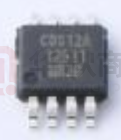
COS12A12511
High Voltage, Single and Dual Supply
SPDT Analog Switch
Features
General Description
■ Single and Dual Supply Operation
The COS12A12511 is a high voltage single
-
±1.5V to ±8V
channel, bidirectional, single-pole double-throw
+3V to +16V
(SPDT) CMOS analog switch. The device can
■ Low ON-State Resistance:
pass signals with swings of 0 to 16 V or -8V to
- 2.8Ω with 16V Supply
+8V. This switch conducts equally well in both
- 3.6Ω with 12V Supply
directions when it is on.
-
- 11Ω with 5V Supply
■ Low Leakage Currents
- 1 nA Off-Leakage at 25oC
- 1 nA On-Leakage at 25oC
■ Fast Switching Speed
tON=70ns, tOFF=50ns (12V Supply)
■ Break-Before-Make Operation
■ Rail-to-Rail Operation
■ TTL/CMOS Logic Compatible
■ Packaging: MSOP8 and SOP8
Pin Diagram
Rev1.0
Copyright@2018 Cosine Nanoelectronics Inc. All rights reserved
The information provided here is believed to be accurate and reliable. Cosine Nanoelectronics assumes
no reliability for inaccuracies and omissions. Specifications described and contained here are subjected
to change without notice on the purpose of improving the design and performance. All of this information
described herein should not be implied or granted for any third party.
www.cosine-ic.com
The COS12A12511 can operate continuously
with a single supply between 3V and 16V or
dual supply between ± 1.5V to ± 8V. It can
handle rail-to-rail analog signals. The OFF/ON
leakage current maximum is only 1nA at 25oC
or 10nA at 85oC. The digital inputs have 0.8V to
2.4V logic thresholds, ensuring TTL/CMOS
logic compatibility when using a +5V supply.
Applications
■
Power routing applications
■
Audio and video signal switching
■
Precision automatic test equipment
■
Relay replacement
■
Automotive applications
■
Sample and hold systems
■
Telecom signal switching
■
Battery power systems
1
�COS12A12511
1. Pin Configuration and Functions
Figure 1 Pin Diagram
Pin Description
PIN
FUNCTION
NO.
NAME
I/O
1
COM
I/O
Common terminal. Can be an input or output
2
NC
I/O
Normally closed terminal. Can be an input or output
3
GND
-
Ground. 0V reference
4
V+
I
Most positive power supply
5
N.C.
-
No connect. Not internally connected
6
IN
I
Logic control input
7
V-
I
Most negative power supply. This pin is only used in
dual-supply applications and should be tied to ground
in single-supply applications.
8
NO
I/O
Normally open terminal. Can be an input or output
2. Ordering Information
Order Number
COS12A12511
COS12A12511SR
www.cosine-ic.com
Package
Package Option
Marking
Information
MSOP8
Tape and Reel, 3000
COS12A12511
SOP8
Tape and Reel, 4000
COS12A12511SR
2
�COS12A12511
3. Product Specification
3.1 Absolute Maximum Ratings (1)
Min
Max
Unit
0
17
V
V+ to GND
-0.3
17
V
V- to GND
-8.5
0.3
V
V- -0.5
V+ + 0.5
V
Continuous current into any terminal
±20
mA
Peak current into any terminal
±50
mA
Continuous power dissipation
560
mW
Parameter
V+ to V-
Analog voltage range (VNC, VNO, VCOM)
Operating junction temperature
-40
+125
°C
Storage temperature
-55
+150
°C
(1) Stresses exceeding the absolute maximum ratings may damage the device. The device may not function or be operable
above the recommended operating conditions and stressing the parts to these levels is not recommended. In addition,
extended exposure to stresses above the recommended operating conditions may affect device reliability. The absolute
maximum ratings are stress ratings only.
3.2 Thermal Data
Parameter
Rating
Unit
206 (MSOP8)
155 (SOP8)
°C/W
Parameter
Rating
Unit
V+
0V ~ 16
V
V-
-8 ~ 0
V
VI/O
V- to V+
V
VIN
0 ~ V+
V
Package Thermal Resistance
3.3 Recommended Operating Conditions
www.cosine-ic.com
3
�COS12A12511
3.4 Electrical Characteristics for ±8V Dual Supply
(Typical values are tested at TA=25 oC, V+=8V±10%, V-=-8V±10%, unless otherwise noted)
Parameter
Symbol
Conditions
Min.
Typ.
Max.
Unit
V+
V
3.2
6
Ω
1.0
3
Ω
50
nA
50
nA
Analog Switch
Analog signal range
VCOM,
VNO, VNC,
On-state resistance
RON
On-state resistance flatness
RON
OFF leakage current
(NO, NC)
ON leakage current (NO, NC)
INO(OFF),
INC(OFF)
INO(ON),
INC(ON)
VVNC or VNO = -4.5V to +4.5V,
ICOM= -10mA
VNC or VNO = -3.3V to +3.3V,
ICOM= -10mA
VNC or VNO = -4.5V to +4.5V,
VCOM = -4.5V to +4.5V
VNC or VNO = -4.5V to +4.5V,
VCOM = open
Digital Control Input (IN)
Input logic high
VIH
5
V+
V
Input logic low
VIL
0
0.8
V
Input leakage current
IIH, IIL
0.05
μA
70
130
ns
50
75
ns
VIN = 0 or V+
Switch Dynamic Characteristics
Turn-on time
tON
Turn-off time
tOFF
Break-Before-Make Delay
(COS4561 only)
tBBM
Charge Injection
Q
NO or NC off capacitance
COFF
COM off-capacitance
(COS4514/COS4515 only)
CCOM
COM On-Capacitance
CCOM
Off-Isolation
VISO
Bandwidth
BW
VNO or VNC=3.3V, RL=300Ω,
CL = 35pF, Figure 1
VNO or VNC=3.3V, RL=300Ω,
CL = 35pF, Figure 1
VNO or VNC=3.3V, RL=300Ω,
CL = 35pF, Figure 2
VNO=VNC=0V, RGEN=0,
CL = 1.0nF, Figure 3
VNC=VNO = 0,
f = 1MHz,
VCOM = 0,
f = 1MHz,
VCOM = VNO, VNC = 0,
f = 1MHz,
RL = 50Ω, CL = 15pF,
VNC = 1VRMS, f = 100kHz
RL = 50Ω, CL = 15pF,
VNC = 1VRMS, f = 100kHz
5
40
ns
-110
pC
15
pF
65
pF
65
pF
-85
dB
100
MHz
Power Supply
V+ supply
current
www.cosine-ic.com
I+
VIN = 0 or V+
0.1
μA
4
�COS12A12511
3.5 Electrical Characteristics for 12V Single Supply
(Typical values are tested at TA=25 oC, V+=11.4V to 12.6V, VINH=5V, VINL=0.8, unless otherwise noted)
Parameter
Symbol
Conditions
Min.
Typ.
Max.
Unit
V+
V
4.0
7.4
Ω
1.5
3
Ω
50
nA
50
nA
Analog Switch
Analog signal range
VCOM,
VNO, VNC,
On-state resistance
RON
On-state resistance flatness
RON
OFF leakage current
(NO, NC)
ON leakage current (NO, NC)
INO(OFF),
INC(OFF)
INO(ON),
INC(ON)
0
VNC or VNO = 0V to 10.8V,
ICOM= -10mA
VNC or VNO = 3.3V to +7V,
ICOM= -10mA
VNC or VNO =0V to 10.8V,
VCOM = 0V to 10.8V
VNC or VNO = 0V to 10.8V,
VCOM = open
Digital Control Input (IN)
Input logic high
VIH
5
V+
V
Input logic low
VIL
0
0.8
V
Input leakage current
IIH, IIL
0.01
μA
70
130
ns
50
75
ns
VIN = 0 or V+
Switch Dynamic Characteristics
Turn-on time
tON
Turn-off time
tOFF
Break-Before-Make Delay
(COS4561 only)
tBBM
Charge Injection
Q
NO or NC off capacitance
COFF
COM off-capacitance
(COS4514/COS4515 only)
CCOM
COM On-Capacitance
CCOM
Off-Isolation
VISO
Bandwidth
BW
VNO or VNC=10V, RL=300Ω,
CL = 35pF, Figure 1
VNO or VNC=10V, RL=300Ω,
CL = 35pF, Figure 1
VNO or VNC=10V, RL=300Ω,
CL = 35pF, Figure 2
VGEN =5V, RGEN=0,
CL = 1.0nF, Figure 3
VNC=VNO = 0,
f = 1MHz,
VCOM = 0,
f = 1MHz,
VCOM = VNO, VNC = 0,
f = 1MHz,
RL = 50Ω, CL = 15pF,
VNC = 1VRMS, f = 100kHz
RL = 50Ω, CL = 15pF,
VNC = 1VRMS, f = 100kHz
5
40
ns
-110
pC
15
pF
65
pF
65
pF
-85
dB
90
MHz
Power Supply
V+ supply
current
www.cosine-ic.com
I+
VIN = 0 or V+
0.1
μA
5
�COS12A12511
3.6 Electrical Characteristics for 5V Single Supply
(Typical values are tested at TA=25 oC, V+=4.5V to 5.5V, VINH=2.4V, VINL=0.8, unless otherwise noted)
Parameter
Symbol
Conditions
Min.
Typ.
Max.
Unit
V+
V
32
Ω
50
nA
50
nA
Analog Switch
Analog signal range
VCOM,
VNO, VNC,
On-state resistance
RON
OFF leakage current
(NO, NC)
INO(OFF),
ON leakage current (NO, NC)
INC(OFF)
INO(ON),
INC(ON)
0
VNC or VNO = 0V to 4.5V,
ICOM= -10mA
VCOM=0V to 4.5V,
VNO or VNC=0V to 4.5V
VCOM=open,
VNO or VNC=0V to 4.5V
11
Digital Control Input (IN)
Input logic high
VIH
2.4
V+
V
Input logic low
VIL
0
0.8
V
Input leakage current
IIH, IIL
0.01
μA
75
130
ns
45
70
ns
VIN = 0 or V+
Switch Dynamic Characteristics
Turn-on time
tON
Turn-off time
tOFF
Break-Before-Make Delay
(COS4561 only)
tBBM
Charge Injection
Q
NO or NC Off Capacitance
COFF
COM Off-Capacitance
(COS4514/COS4515 only)
CCOM
COM On-Capacitance
CCOM
Off-Isolation
VISO
Bandwidth
BW
VNO or VNC=3V, RL=300Ω,
CL = 35pF, Figure 1
VNO or VNC=3V, RL=300Ω,
CL = 35pF, Figure 1
VNO or VNC=3V, RL=300Ω,
CL = 35pF, Figure 2
VGEN =2V, RGEN=0,
CL = 1.0nF, Figure 3
VNC=VNO = 0,
f = 1MHz,
VCOM = 0,
f = 1MHz,
VCOM = VNO, VNC = 0,
f = 1MHz,
RL = 50Ω, CL = 15pF,
VNC = 1VRMS, f = 100kHz
RL = 50Ω, CL = 15pF,
VNC = 1VRMS, f = 100kHz
5
40
ns
-40
pC
15
pF
65
pF
65
pF
-85
dB
60
MHz
Power Supply
V+ supply
current
www.cosine-ic.com
I+
VIN = 0 or V+
0.1
μA
6
�COS12A12511
4. Test Circuits and Timing Diagrams
Figure 1. Switching Time
Figure 2. Break-Before-Make Interval
Figure 3. Charge Injection
www.cosine-ic.com
7
�COS12A12511
5. Package Information
5.1 MSOP8 (Package Outline Dimensions)
5.2 SOP8 (Package Outline Dimensions)
www.cosine-ic.com
8
�