LN2266
Super-Small Package PWM Control Step-up Switching Regulator
■ General Description
The LN2266
is a compact, high efficiency, and
High supply capability to deliver 3.3V 300mA with1
alkaline cell or deliver 5V 1100mA with 1 Li-ion Cell
low
voltage step-up DC/DC converter with an Adaptive Current
Mode PWM control loop, includes an error amplifier,
ramp generator, comparator, switch pass element and
17µA quiescent (switch-off) supply current
0.01µA shutdown mode supply current
Providing flexibility for using internal and external
power switches
driver in which providing a stable and high efficient
operation over a wide range of load currents. It operates in
Output
voltage:
settable
to
between
2.0V
to
6.0V ,accuracy of 2%
stable waveforms without external compensation.
■ Applications
The low start-up input voltage below 0.9V makes LN2266
suitable for 1 to 4 battery cells applications of providing up
to 1100mA output current. Besides, the 17µA low
quiescent current together with high efficiency maintains
long battery lifetime. The output voltage is set with two
external resistors. Both internal 2.5A switch and driver for
driving external power devices (NMOS or NPN) are
provided.
■ Features
MP3
PDA
DSC
LCD panel
RF-Tags
Portable
Wireless equipment
instrument
■ Package
0.9V(Iout=1mA) Low start-up input voltage
1000kHz fixed switching frequency
90% efficiency
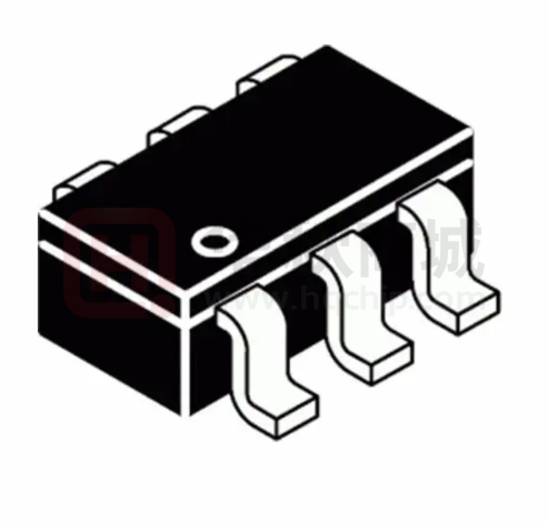
SOT-23-6L
SOT-89-5L
■ Ordering Information
LN2266P①②③④
Designator
①
②
Symbol
Description
Designator
Symbol
Description
M
SOT-23-6L
SOT-89-5L
A
CE with EXT
B
CE without EXT
P
1
Reference accuracy:±1%
R
Embossed Tape :Standard Feed
2
Reference accuracy:±2%
L
Embossed Tape : Reverse Feed
4
Reference accuracy:±4%
③
④
■ Pin Configuration
Rev.1.0 — Dec. 20, 2011
1
www.natlinear.com
�LN2266
■ Pin Assignment
Pin Mumber
Pin Name
Function
SOT-23-6
SOT-89-5
1
1
CE
Chip enable
2
-
NC
Floating or connected to GND
3
5
GND
4
4
LX
5
2
VDD
6
3
FB
Ground
Pin for switching
Input positive power pin of LN2266
Feedback input pin
■ Marking Rule
1
2
3
SOT-23-6L, SOT-89-5L
Represents the product name
Symbol
Product Name
A
LN2266P****
Represents the type of regulator
Symbol
A
B
Type
CE with EXT
CE without EXT
Represents the accuracy of reference voltage
Symbol
Reference Accuracy
1
1%
2
2%
4
4%
④ Represents the assembly lot No.
0-9,A-Z; 0-9,A-Z mirror writing,repeated(G,I,J,O,Q,W exception)
Rev.1.0 — Dec. 20, 2011
2
www.natlinear.com
�LN2266
■ Function Block Diagram
■ Absolute Maximum Ratings
Parameter
Input voltage
Output voltage
LX pin Switch Current
Power dissipation
PD
Symbol
Maximum Rating
VDD
Vss-0.3~Vss+7
VOUT
Vss-0.3~Vss+7
VLX
Vss-0.3~Vss+7
ILX
2.5
SOT-23-6
150
SOT-89-5
500
Operating ambient temperature
Topr
-40~+80
Storage ambient temperature
Tstg
-40~+125
Unit
V
A
mW
℃
Caution : The absolute maximum ratings are rated values exceeding which the product could suffer physical damage.
These values must therefore not be exceeded under any conditions.
Rev.1.0 — Dec. 20, 2011
3
www.natlinear.com
�LN2266
■ Typical Application Circuit
Circuit 1. LN2266 Typical Application for Portable Instruments
Circuit 2. LN2266 for multi-output Application
Rev.1.0 — Dec. 20, 2011
4
www.natlinear.com
�LN2266
■ Electrical Characteristics
(VIN=1.5V,VDD=3.3V,ILoad =0,Ta=25℃, unless otherwise noted)
Item
Symbol
Condition
Min.
Typ.
Max.
0.9
1.00
Unit
Operation start voltage
VST
IOUT=1mA
-
VDD supply voltage
VDD
VDD pin voltage
2
Shut down current
IOFF
CE=0,VIN=4.5V
-
0.01
1
µA
Switch-off Current
Iswitch-off
VIN=6V
-
17
25
µA
6
V
Continuous Switching Current
Iswitch
VIN=CE=3.3V,VFB=GND
-
500
-
μA
No load Current
Ino-load
VIN=1.5V,VOUT=3.3V
-
56
-
µA
Vref
Close Loop Vdd=3.3V
1.225
1.25
1.275
V
Feedback Reference Voltage
Switching Frequency
Fs
Vdd=3.3V
800
1000
1250
KHz
Dmax
Vdd=3.3V
70
75
80
%
Vdd=3.3V
-
0.18
0.25
Ω
Vdd=3.3V
2.3
2.5
2.7
A
EXT on resistance to VDD
Vdd=3.3V
-
4
8.0
Ω
EXT on resistance to GND
Vdd=3.3V
-
2.15
8.0
Ω
Maximum Duty
LX on resistance
Current Limit Setting
Ilimit
Line Regulation
ΔVline
Vin=3.5~6V,IL=1mA
-
0.25
5
mV/V
Load Regulation
ΔVload
VIN=2.5V,IL=1~100mA
-
0.5
-
mV/mA
VDD=3.3V
0.4
0.8
1.2
V
CE pin Trip level
Temperature Stability for Vout
Ts
-
50
-
Ppm/℃
Thermal Shut down Hysterises
ΔTsd
-
10
-
℃
■ Test Circuits
Rev.1.0 — Dec. 20, 2011
5
www.natlinear.com
�LN2266
■ Typical Performance Characteristics
1.
Efficiency vs. Output Current
3.
Switching Frequency vs. Vdd pin Voltage
5.
Transient Response
Rev.1.0 — Dec. 20, 2011
2. Supply Current vs. Input Voltage
6
4.
LX pin wave form & Output Ripple
6.
Output Voltage vs. Temperature
www.natlinear.com
�LN2266
7.VIN VS The Max Output Current ( VOUT=5.0V)
■ Package Information
SOT-23-6L
Rev.1.0 — Dec. 20, 2011
7
www.natlinear.com
�LN2266
SOT-89-5L
Rev.1.0 — Dec. 20, 2011
8
www.natlinear.com
�LN2266
Rev.1.0 — Dec. 20, 2011
9
www.natlinear.com
�
很抱歉,暂时无法提供与“LN2266PB2MR-G”相匹配的价格&库存,您可以联系我们找货
免费人工找货- 国内价格
- 5+0.56798
- 50+0.44356
- 150+0.38135
- 500+0.33470
- 3000+0.29733
- 6000+0.27864