SW076R68E7T
N-channel Enhanced mode TO-252 MOSFET
Features
⚫
⚫
⚫
⚫
⚫
⚫
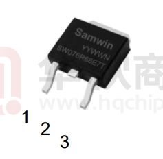
TO-252
High ruggedness
Low RDS(ON) (Typ 8mΩ)@VGS=10V
Low Gate Charge (Typ 80nC)
Improved dv/dt Capability
100% Avalanche Tested
Application:Synchronous Rectification,
Li Battery Protect Board, Inverter
BVDSS : 68V
ID
: 85A
RDS(ON) : 8mΩ
1
2
2
3
1
1. Gate 2.Drain 3.Source
General Description
3
This power MOSFET is produced with advanced technology of SAMWIN.
This technology enable the power MOSFET to have better characteristics,
including fast switching time, low on resistance, low gate charge and especially
excellent avalanche characteristics.
Order Codes
Item
Sales Type
Marking
Package
Packaging
1
SW D 076R68E7T
SW076R68E7T
TO-252
REEL
Value
Unit
Drain to source voltage
68
V
Continuous drain current (@TC=25oC)
85*
A
Continuous drain current (@TC=100oC)
60*
A
340
A
± 20
V
Absolute maximum ratings
Symbol
VDSS
Parameter
ID
IDM
Drain current pulsed
(note 1)
VGS
Gate to source voltage
EAS
Single pulsed avalanche energy
(note 2)
182
mJ
EAR
Repetitive avalanche energy
(note 1)
18
mJ
dv/dt
Peak diode recovery dv/dt
(note 3)
5
V/ns
Total power dissipation (@TC=25oC)
125
W
Derating factor above 25oC
1.0
W/oC
-55 ~ + 150
oC
Value
Unit
1.0
oC/W
PD
TSTG, TJ
Operating junction temperature & storage temperature
*. Drain current is limited by junction temperature.
Thermal characteristics
Symbol
Rthjc
Parameter
Thermal resistance, Junction to case
Copyright@ Semipower Technology Co., Ltd. All rights reserved.
May.2022. Rev. 0.6
1/6
�SW076R68E7T
Electrical characteristic ( TJ = 25oC unless otherwise specified )
Symbol
Parameter
Test conditions
Min.
Typ.
Max.
Unit
Off characteristics
BVDSS
Drain to source breakdown voltage
VGS=0V, ID=250uA
ΔBVDSS
/ ΔTJ
Breakdown voltage temperature
coefficient
ID=250uA, referenced to 25oC
IDSS
Drain to source leakage current
68
V
V/oC
0.04
VDS=68V, VGS=0V
1
uA
VDS=54V, TJ=125oC
50
uA
Gate to source leakage current, forward
VGS=20V, VDS=0V
100
nA
Gate to source leakage current, reverse
VGS=-20V, VDS=0V
-100
nA
4
V
9.1
mΩ
IGSS
On characteristics
VGS(TH)
Gate threshold voltage
RDS(ON)
Drain to source on state resistance
Gfs
Forward transconductance
VDS=VGS, ID=250uA
2
VGS=10V, ID=40A,TJ=25oC
8.0
VGS=10V, ID=40A,TJ=125oC
13
mΩ
VDS=5V, ID=40A
48
S
Dynamic characteristics
Ciss
Input capacitance
Coss
Output capacitance
Crss
Reverse transfer capacitance
td(on)
Turn on delay time
tr
td(off)
tf
Rising time
Turn off delay time
3704
VGS=0V, VDS=34V, f=1MHz
231
pF
219
22
VDS=34V, ID=30A, RG=4.7Ω,
VGS=10V
(note 4,5)
61
ns
67
Fall time
28
Qg
Total gate charge
80
Gate-drain charge
VDS=54V, VGS=10V, ID=30A ,
IG=3mA
(note 4,5)
Qgs
Gate-source charge
Qgd
Rg
Gate resistance
VDS=0V, Scan F mode
3.5
20
nC
31
Ω
Source to drain diode ratings characteristics
Symbol
Parameter
IS
Continuous source current
ISM
VSD
Test conditions
Min.
Typ.
Max.
Unit
85
A
Pulsed source current
Integral reverse p-n Junction
diode in the MOSFET
340
A
Diode forward voltage drop.
IS=45A, VGS=0V
1.4
V
trr
Reverse recovery time
Qrr
Reverse recovery charge
IS=30A, VGS=0V,
dIF/dt=100A/us
35
ns
44
nC
※. Notes
1.
Repeatitive rating : pulse width limited by junction temperature.
2.
L =0.5mH, IAS =27A, VDD=50V, RG=25Ω, Starting TJ = 25oC
3.
ISD ≤30A, di/dt = 100A/us, VDD ≤ BVDSS, Staring TJ =25oC
4.
Pulse Test : Pulse Width ≤ 300us, duty cycle ≤ 2%.
5.
Essentially independent of operating temperature.
Copyright@ Semipower Technology Co., Ltd. All rights reserved.
May.2022. Rev. 0.6
2/6
�SW076R68E7T
Fig. 1. On-state characteristics
Fig. 2. Transfer Characteristics
Fig. 3. On-resistance variation vs.
drain current and gate voltage
Fig. 4. On-state current vs. diode
forward voltage
Fig 5. Breakdown voltage variation
vs. junction temperature
Fig. 6. On-resistance variation
vs. junction temperature
Copyright@ Semipower Technology Co., Ltd. All rights reserved.
May.2022. Rev. 0.6
3/6
�SW076R68E7T
Fig. 7. Gate charge characteristics
Fig. 9. Maximum safe operating area
Fig. 8. Capacitance Characteristics
Fig. 10. Maximum drain current
vs. case temperature
Fig. 11. Transient thermal response curve
Copyright@ Semipower Technology Co., Ltd. All rights reserved.
May.2022. Rev. 0.6
4/6
�SW076R68E7T
Fig. 12. Gate charge test circuit & waveform
Fig. 13. Switching time test circuit & waveform
VDS
90%
RL
RGS
VDS
VDD
VIN
10VIN
DUT
10%
10%
td(on)
tr
tON
td(off)
tf
tOFF
Fig. 14. Unclamped Inductive switching test circuit & waveform
Copyright@ Semipower Technology Co., Ltd. All rights reserved.
May.2022. Rev. 0.6
5/6
�SW076R68E7T
Fig. 15. Peak diode recovery dv/dt test circuit & waveform
DUT
+ V
DS
10V
VGS (DRIVER)
L
IS
di/dt
IS (DUT)
IRRM
VDS
RG
Diode reverse current
VDD
Diode recovery dv/dt
Same type
as DUT
10VGS
VDS (DUT)
*. dv/dt controlled by RG
*. Is controlled by pulse period
VDD
VF
Body diode forward voltage drop
DISCLAIMER
* All the data & curve in this document was tested in SEMIPOWER TESTING & APPLICATION CENTER.
* This product has passed the PCT,TC,HTRB,HTGB,HAST,PC and Solderdunk reliability testing.
* Qualification standards can also be found on the Web site (http://www.semipower.com.cn)
* Suggestions for improvement are appreciated, Please send your suggestions to samwin@samwinsemi.com
Copyright@ Semipower Technology Co., Ltd. All rights reserved.
May.2022. Rev. 0.6
6/6
�