物料型号:UMW AO6604
器件简介:AO6604是一款结合了先进的沟槽MOSFET技术和低电阻封装的产品,提供极低的RDS(ON),非常适合用于负载开关和电池保护应用。
引脚分配:
- N-Channel:G1, D1, S2, S1, D2, G2
- P-Channel:与N-Channel相同,但极性相反
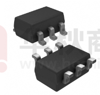
- 封装类型:SOT23-6
参数特性:
- N-Channel和P-Channel的最大漏源电压(VDS)分别为20V和-20V。
- N-Channel的RDS(ON)在不同VGS下的值分别为:<65 mΩ (VGS=4.5V), <75 mΩ (VGS=2.5V), <100 mΩ (VGS=1.8V)。
- P-Channel的RDS(ON)在不同VGS下的值分别为:<75 mΩ (VGS=-4.5V), <95 mΩ (VGS=-2.5V), <115 mΩ (VGS=-1.8V)。
功能详解:
- 器件提供了N通道和P通道MOSFET,用于不同的电路控制需求。
- 器件的热特性包括最大结到环境的热阻(RaJA)和最大结到引线的热阻(RaJL)。
应用信息:
- 适用于负载开关和电池保护等应用。
封装信息:
- 封装类型为SOT23-6,提供了详细的封装尺寸和标记信息。
订购信息:
- 订购代码:UMW AO6604
- 封装:SOT23-6
- 基础数量:3000
- 交付方式:带卷装