microSplatch™
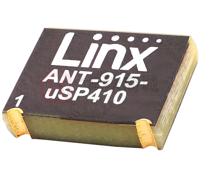
ANT-915-uSP410
915 MHz LPWA Weatherproof Antenna
The microSplatch™ uSP410 915 MHz antenna is a surface-mount monopole antenna for embedded Sub-1 GHz and
low-power, wide-area (LPWA) applications including LoRaWAN®, remote controls, and ISM applications in the 902
MHz to 928 MHz band.
uSP410 series monopole antennas use a grounded-line technique to achieve outstanding
performance in a compact surface-mount package. The uSP410 series exhibits low proximity effect, making it a good
embedded antenna choice for devices typically subject to nearby interferers.
uSP410 series antennas are available in tape and reel packaging and are designed for reflow-solder mounting directly
to a printed circuit board for high- volume applications.
FEATURES
APPLICATIONS
• Performance at 902 MHz to 928 MHz
– VSWR: ≤ 2.7
– Peak Gain: 0.9 dBi
– Efficiency: 27%
• Low-power, wide-area (LPWA) applications
– LoRaWAN®
– Sigfox®
– WiFi HaLow™
• Omnidirectional radiation pattern
• Compact package
– 13.2 mm x 9.1 mm x 2.9 mm
• Remote sensing, monitoring and control
– Security systems
– Industrial machinery
• Direct surface-mount PCB attachment
• Internet of Things (IoT) devices
• Reflow- or hand-solder assembly
• ISM applications
• Resistant to proximity effect from nearby
interferers
• Smart Home networking
• Hand-held devices
• Excellent performance with small ground plane
(38 mm x 84 mm)
ORDERING INFORMATION
Part Number
Description
ANT-915-uSP410
915 MHz microSplatch antenna on tape and reel (1000 per reel)
AEK-915-uSP410
915 MHz microSplatch antenna evaluation kit
Available from Linx Technologies and select distributors and representatives.
DATA AND DEVICES / MICROSPLATCH™ ANT-915-USP410
�TABLE 1. ELECTRICAL SPECIFICATIONS
ANT-915-uSP410
VSWR (max)
Peak Gain (dBi)
Average Gain (dBi)
Efficiency (%)
Polarization
Radiation
Max Power
Wavelength
Electrical Type
Impedance
Connection
Weight
Dimensions
Operating Temperature Range
ESD Sensitivity
902 MHz to 928 MHz
2.7
0.9
-5.8
27
Linear
Omnidirectional
5W
1/4-wave
Monopole
50 Ω
Surface-mount
0.6 g (0.02 oz)
13.2 mm x 9.1 mm x 2.9 mm (0.52 in x 0.36 in x 0.11 in)
-40 °C to +130 °C
NOT ESD sensitive. As a best practice, Linx may use ESD packaging.
Electrical specifications and plots measured with a 38 mm x 84 mm (1.5 in x 3.3 in) reference ground plane.
VSWR
Figure 1 provides the voltage standing wave ratio (VSWR) across the antenna bandwidth. VSWR describes the power
reflected from the antenna back to the radio. A lower VSWR value indicates better antenna performance at a given
frequency. Reflected power is also shown on the right-side vertical axis as a gauge of the percentage of transmitter
power reflected back from the antenna.
5
928
902
VSWR response typically shifts lower in frequency when the antenna is in proximity to an enclosure or printed circuit
board. By allowing for this shift in the antenna design, the need for complex matching circuits is reduced.
VSWR
4
30
3
20
2
10
1
0
900
905
910
915
Frequency (MHz)
920
925
930
Reflected Power (%)
40
Figure 1. ANT-915-uSP410 VSWR
DATA AND DEVICES / MICROSPLATCH™ ANT-915-USP410
2
�RETURN LOSS
0
928
902
The peak gain across the antenna bandwidth is shown in Figure 2. Peak gain represents the maximum antenna input
power concentration across 3-dimensional space, and therefore peak performance at a given frequency, but does not
consider any directionality in the gain pattern.
-2
Return Loss (dB)
-4
-6
-8
-10
-12
-14
-16
-18
-20
900
905
910
915
Frequency (MHz)
920
925
930
Figure 2. ANT-915-uSP410 Return Loss
PEAK GAIN
Peak Gain (dBi)
5
928
902
The peak gain across the antenna bandwidth is shown in Figure 3. Peak gain represents the maximum antenna input
power concentration across 3-dimensional space, and therefore peak performance at a given frequency, but does not
consider any directionality in the gain pattern.
0
-5
-10
900
905
910
915
Frequency (MHz)
920
925
930
Figure 3. ANT-915-uSP410 Peak Gain
DATA AND DEVICES / MICROSPLATCH™ ANT-915-USP410
3
�AVERAGE GAIN
Average Gain (dBi)
5
928
902
Average gain (Figure 4), is the average of all antenna gain in 3-dimensional space at each frequency, providing an
indication of overall performance without expressing antenna directionality.
0
-5
-10
900
905
910
915
Frequency (MHz)
920
925
930
Figure 4. ANT-915-uSP410 Average Gain
RADIATION EFFICIENCY
100
928
902
Radiation efficiency (Figure 5), shows the ratio of power delivered to the antenna relative to the power radiated at
the antenna, expressed as a percentage, where a higher percentage indicates better performance at a given
frequency.
90
80
Efficiency (%)
70
60
50
40
30
20
10
0
900
905
910
915
Frequency (MHz)
920
925
930
Figure 5. ANT-915-uSP410 Radiation Efficiency
DATA AND DEVICES / MICROSPLATCH™ ANT-915-USP410
4
�PRODUCT DIMENSIONS
13.2 mm
(0.52 in)
9.1 mm
(0.36 in)
1
2.9 mm
(0.11 in)
ANT-fffuSP410
10.2 mm
(0.40 in)
Figure 6. uSP410 Series Antenna Dimensions
PRODUCT SIGNALS
The signal definitions for the uSP410 are provided in Figure 7.
Function
Description
Rx/Tx
Castellation marked as “1”
GND
Unmarked castellation
13.2
(0.52
Figure 7. uSP410 Series Pin-Out Table
PROXIMITY EFFECT
Wireless devices are often designed based on antenna performance measured on an evaluation9.1
board.
mm
In practice, however, many wireless devices are used in the presence of materials near the antenna
were not
(0.36which
in)
present during evaluation. These materials, such as batteries, components on the PCB, or even a person’s body or
hand1, can cause a shift in the frequency performance of the antenna, resulting in less than optimal device
performance. The shift in the frequency performance can be quite dramatic, especially for monopole (1/4 wavelength)
antennas.
1
ANT
uSP
The uSP410 Series antennas are designed to help reduce the impact of nearby objects on the performance of the
antenna by using a grounded line technique to reduce the overall length of the antenna radiator to provide wider
bandwidth for better immunity to frequency shifts, while using a multilayer PCB to maintain a lower profile and small
size. Matching components can be added, if necessary, to mitigate larger proximity effects from features like metal
shields or enclosures.
10.2
(0.40
DATA AND DEVICES / MICROSPLATCH™ ANT-915-USP410
5
�RADIATION PATTERNS
Radiation patterns provide information about the directionality and 3-dimensional gain performance of the antenna
by plotting gain at specific frequencies in three orthogonal planes. Antenna radiation patterns are shown in Figure 8
using polar plots covering 360 degrees. The antenna graphic provides reference to the plane of the plots below it.
Note: when viewed with typical PDF viewing software, zooming into radiation patterns is possible to reveal fine detail.
XZ-Plane Gain
YZ-Plane Gain
XY-Plane Gain
902 MHZ TO 928 MHZ ( 915 MHZ)
34
35
33
32
31
30
29
28
36 5
0
-5
-10
-15
-20
-25
-30
-35
-40
-45
-50
1
2
3
4
34
5
33
6
32
7
31
8
27
26
30
9
29
10
28
11
27
12
25
13
24
21
20
19
18
17
1
2
3
4
34
5
6
31
8
30
9
29
10
28
11
27
12
13
14
23
15
22
XZ-Plane Gain
32
7
24
16
21
20
19
18
17
35
33
25
15
22
36 5
0
-5
-10
-15
-20
-25
-30
-35
-40
-45
-50
26
14
23
35
16
YZ-Plane Gain
36 5
0
-5
-10
-15
-20
-25
-30
-35
-40
-45
-50
1
2
3
4
5
6
7
8
9
10
11
26
12
25
13
24
14
23
15
22
21
20
19
18
17
16
902 MHz
915 MHz
930 MHz
XY-Plane Gain
Figure 8. ANT-915-uSP410 Radiation Patterns
DATA AND DEVICES / MICROSPLATCH™ ANT-915-USP410
6
�RECOMMENDED LAYOUT
The recommended printed circuit board (PCB) layout for the uSP410 antenna series is shown in Figure 9. This
layout is used for the uSP410 series evaluation board which is available for purchase as listed under Ordering
Information. Contact Linx for availability of PCB layout design files.
The recommended layout includes a matching network, ground plane and PCB transmission line from the
1.5 mm to 2 mm
antenna to the matching network, and to the connector or radio circuitry.
(0.06 in to 0.08 in)
Top layer keep out zone
ANTENNA PLACEMENT
Antenna placement should be such that the feedline (marked 1) is near to the corner of the ground plane to
allow a maximum diagnonal ground plane length for the antenna counterpoise.
The antenna should have a minimum of 5 mm of clearance from circuitry and ground plane on non-attaching
sides, and no ground plane or circuitry underneath the antenna.
MATCHING NETWORK
Linx recommends inclusion of at least a 3-element, surface mount pi matching network of two parallel capacitors,
(C1, C2) and one serial inductor, (L1) in all designs (Figure 10). Surface mount components should be 0603 size. 0402
size components are also supported. The uSP410 series antennas, as designed, do not require matching, but matching
may improve end-product antenna performance depending on the effects of the enclosure, PCB and other electronic
components. If no matching is necessary, the serial element may be populated with a zero-ohm resistor and no
components in the two capacitor positions. This is the configuration of the Linx evaluation board as supplied.
Linx believes in wireless made simple® and offers matching network design support.
ANT-fff1 uSP410
C2
C2
Pi matching circuit
L1
L1
50 Ω microstrip feedline
on top layer ANTENNA
C1
L1
Ground
plane on bottom layer
for counterpoise
C2
C1
2-Element
L1
C1
GND
C1
GND
Figure 9. Linx uSP410 Series Recommended Layout.
3-Element
L1
C1
4-Element
C1
C2
C2
L1
L2
Figure 10. Matching Network Recommendation
DATA AND DEVICES / MICROSPLATCH™ ANT-915-USP410
7
�RECOMMENDED PCB FOOTPRINT
Figure 11 shows the recommended printed circuit board footprint and spacing for uSP410 series antennas. The
footprint recommendation should be used in conjunction with the recommended layout configuration shown in
Figure 9.
10.2 mm
(0.40 in)
No ground plane or traces
under antenna.
2x Solder pads
2.0 mm x 2.5 mm
(0.08 in x 0.10 in)
C2
L1
ne
50 Ω microstrip feedline
on top layer
Ground plane on bottom layer
for counterpoise
C1
Ground plane area =
38 mm x 84 mm (1.5 in x 3.3 in)
om layer
Figure 11. uSP410 Series Antenna Placement on PCB.
GROUND PLANE
The ANT-915-uSP410 is a 1/4 wave monopole antenna, and requires a ground plane on the PCB to which it is mounted.
Linx recommends a minimum 38 mm x 84 mm or larger ground plane. The uSP410 should be mounted at the top
edge of the ground plane, (See Figure 9) and none of the ground plane should be underneath the antenna.
Other ground plane sizes and antenna mounting locations are possible. Simulated performance data for different
ground plane sizes can be found in the application note, microSplatch™ uSP410 Series Ground Plane Optimization, on
the Linx website. Linx offers PCB design reviews to help optimize solution performance.
TRANSMISSION LINES FOR EMBEDDED ANTENNAS
For most designs, Linx recommends a microstrip transmission line for the uSP410 series. A microstrip transmission
line is a PCB trace that runs over a ground plane to maintain the characteristic impedance for optimal signal transfer
between the antenna and radio circuitry. Linx designs all antennas with a characteristic impedance of 50 Ω.
Important practices to observe when designing a transmission line are:
• Keep all transmission lines to a minimum length for best signal performance
• Use RF components that also operate at a 50 Ω impedance
• If the radio is not on the same PCB as the antenna, the microstrip should be terminated in a connector,
as exemplified on the uSP410 evaluation board, enabling a shielded cable to complete the antenna connection
to the radio
• For designs subject to significant electromagnetic interference, a coplanar waveguide transmission line may be
used on the PCB
The design of a PCB transmission line can be aided by many commercially available software packages which can
calculate the correct transmission line width and gap dimensions based upon the PCB thickness and dielectric
constant used. Linx offers PCB design reviews to help optimize solution performance.
DATA AND DEVICES / MICROSPLATCH™ ANT-915-USP410
8
�REFLOW SOLDER PROFILE
The uSP410 series antennas use a typical RoHS solder reflow profile. Refer to application note, AN-00504,
on the Linx website for more information.
TAPE AND REEL PACKAGING
Figure 12 shows the dimensions of the tape in which the uSP410 series are packaged. Reel dimensions are provided in
Figure 13.
Tape Dimensions
P5
P3
D1
P4
D2
P2
ANT-fffuSP410
W
F
P1
T2
T3
T4
Figure 12. Tape Specifications for the uSP410 Series Antenna
Symbol
Dimension
(mm)
Tolerance
D1
1.50
± 0.10
D2
1.50
± 0.10
F
13.00
± 0.10
P1
16.00
± 0.10
P2
11.50
± 0.10
P3
1.75
± 0.10
P4
4.00
± 0.10
P5
2.00
± 0.10
T2
0.35
± 0.05
T3
9.45
± 0.10
T4
3.20
± 0.10
W
24.00
± 0.30
W1
E
C
B
A
Reel Dimensions
Symbol
uSP410
Unit
QTY per reel
1,000
pcs
Tape width
24.00
mm
A
Ø 330 ±1
mm
B
Ø 100 ±0.5
mm
C
Ø 13.00 ±0.2
mm
E
2.2 ±0.5
mm
W
24 ±0.5
mm
W1
28.4 ±0.2
mm
W
Figure 13. Reel Specifications for the uSP410 Series Antenna
DATA AND DEVICES / MICROSPLATCH™ ANT-915-USP410
9
�RADIATION PATTERNS
Radiation patterns provide information about the directionality and 3-dimensional gain performance of the antenna
by plotting gain at specific frequencies in three orthogonal planes. Antenna radiation patterns for a free space
orientation are shown in Figure 16 using polar plots covering 360 degrees. The antenna graphic at the top of the page
provides reference to the plane of the column of plots below it. Note: when viewed with typical PDF viewing software,
zooming into radiation patterns is possible to reveal fine detail.
RADIATION PATTERNS - STRAIGHT, NO GROUND PLANE
XZ-Plane Gain
YZ-Plane Gain
XY-Plane Gain
902 MHZ TO 930 MHZ ( 915 MHZ)
34
35
33
32
31
30
29
28
36 5
0
-5
-10
-15
-20
-25
-30
-35
-40
-45
-50
1
2
3
4
34
5
33
6
32
7
31
8
27
26
30
9
29
10
28
11
27
12
25
13
24
21
20
19
18
17
1
2
3
4
34
5
6
30
9
29
10
28
11
27
12
13
14
15
22
XZ-Plane Gain
31
8
23
16
32
7
24
21
20
19
18
17
35
33
25
15
22
36 5
0
-5
-10
-15
-20
-25
-30
-35
-40
-45
-50
26
14
23
35
16
YZ-Plane Gain
36 5
0
-5
-10
-15
-20
-25
-30
-35
-40
-45
-50
1
2
3
4
5
6
7
8
9
10
11
26
12
13
25
24
14
23
15
22
21
20
19
18
XY-Plane Gain
17
16
902 MHz
915 MHz
930 MHz
Figure 16. Radiation Patterns for ANT-915-IPW1-RPS, Straight
PACKAGING INFORMATION
The ANT-915-IPW1-RPS antenna is packaged in a clear plastic bag. Distribution channels may offer alternative
packaging options.
DATA AND DEVICES / MICROSPLATCH™ ANT-915-USP410
10
�TE TECHNICAL SUPPORT CENTER
USA:
+1 (800) 522-6752
Canada:
+1 (905) 475-6222
Mexico:
+52 (0) 55-1106-0800
Latin/S. America:
+54 (0) 11-4733-2200
Germany:
+49 (0) 6251-133-1999
UK:
+44 (0) 800-267666
France:
+33 (0) 1-3420-8686
Netherlands:
+31 (0) 73-6246-999
China:
+86 (0) 400-820-6015
te.com
TE Connectivity, TE, TE connectivity (logo), Linx and Linx Technologies are trademarks owned or licensed by the TE Connectivity Ltd. family of companies. All other logos,
products and/or company names referred to herein might be trademarks of their respective owners.
The information given herein, including drawings, illustrations and schematics which are intended for illustration purposes only, is believed to be reliable. However,
TE Connectivity makes no warranties as to its accuracy or completeness and disclaims any liability in connection with its use. TE Connectivity‘s obligations shall only be as
set forth in TE Connectivity‘s Standard Terms and Conditions of Sale for this product and in no case will TE Connectivity be liable for any incidental, indirect or consequential
damages arising out of the sale, resale, use or misuse of the product. Users of TE Connectivity products should make their own evaluation to determine the suitability of each
such product for the specific application.
TE Connectivity warrants to the original end user customer of its products that its products are free from defects in material and workmanship. Subject to conditions and
limitations TE Connectivity will, at its option, either repair or replace any part of its products that prove defective because of improper workmanship or materials. This limited
warranty is in force for the useful lifetime of the original end product into which the TE Connectivity product is installed. Useful lifetime of the original end product may vary but
is not warrantied to exceed one (1) year from the original date of the end product purchase.
©2022 TE Connectivity. All Rights Reserved.
09/22 Original
DATA AND DEVICES / MICROSPLATCH™ ANT-915-USP410
�