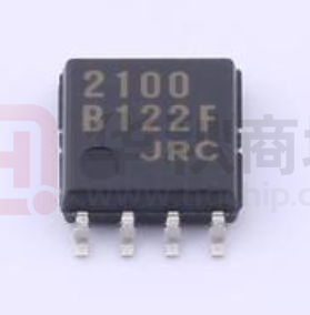
NJM2100
DUAL OPERATIONAL AMPLIFIER
■ GENERAL DESCRIPTION
The NJM2100 is a low voltage operation and low saturation output
voltage ( ±2.0VP-P at supply voltage ±2.5V ) operational amplifier. It is
suitable for digital audio apparatus such as handy type CD, radio
cassette CD, and portable DAT that are required 5V single supply
operation and high output voltage.
■ FEATURES
● Single Supply Operation
● Operating Voltage
● Low Saturation Output Voltage
● High Slew Rate
● Package Outline
■ PACKAGE OUTLINE
NJM2100D
( DIP8 )
NJM2100L
( SIP8 )
NJM2100M
( DMP8 )
NJM2100E
( SOP8 )
( ±1.0V~±3.5V )
( 4V/μs typ. )
DIP8, SIP8, DMP8, SSOP8
SOP8 JEDEC 150mil
● Bipolar Technology
NJM2100V
( SSOP8 )
■ PIN CONFIGURATION
( Top View )
1
2
8
A
7
B
3
A
4
B
6
5
1
NJM2100D
NJM2100M
NJM2100E
NJM2100V
2
3
4
5
6
NJM2100L
7
8
PIN
FUNCTION
1. A OUTPUT
2. A –INPUT
3. A +INPUT
4. V5. B +INPUT
6. B –INPUT
7. B OUTPUT
8. V+
■ EQUIVALENT CIRCUIT ( 1/2 Shown )
V+
- INPUT
+ INPUT
OUTPUT
V-
Ver.2011-12-12
-1-
�NJM2100
■ ABSOLUTE MAXIMUM RATINGS
( Ta=25˚C )
PARAMETER
Supply Voltage
Differential Input Voltage
Input Voltage
SYMBOL
V+/VVID
VIC
Power Dissipation
PD
Operating Temperature Range
Storage Temperature Range
Topr
Tstg
RATINGS
± 3.5
±7
± 3.5
( DIP8 ) 500
( DMP8 ) 300
(SOP8) 300
( SSOP8 ) 250
( SIP8 ) 800
-40~+85
-40~+125
UNIT
V
V
V
mW
˚C
˚C
■ ELECTRICAL CHARACTERISTICS
( Ta=25˚C,V+=5V )
PARAMETER
Input Offset Voltage
Input Bias Current
Large Signal Voltage Gain
Maximum Output Voltage Swing
Input Common Mode Voltage Range
Common Mode Rejection Ratio
Supply Voltage Rejection Ratio
Operating Current
Slew Rate
Gain Bandwidth Product
SYMBOL
VIO
IIB
AV
VOM
VICM
CMR
SVR
ICC
SR
GB
TEST CONDITION
RS≤10kΩ
RL≥10kΩ
RL≥2.5kΩ
VIN=0,RL=∞
AV=1,VIN=±1V
f=10kHz
MIN.
60
±2
± 1.5
60
60
-
TYP.
1
100
80
± 2.2
74
80
3.5
4
12
MAX.
6
300
5
-
UNIT
mV
nA
dB
V
V
dB
dB
mA
V/μs
MHz
( Note1 ) Applied circuit voltage gain is desired to operate within the range of 3dB to 30 dB.
( Note2 ) Special care being required for input common mode voltage range and the oscillation due to the capacitive load when operating on voltage follower.
( Note3 ) Special care being required for the oscillation, yet having the gain when the supply voltage is applied at more than 5V ( single supply voltage 5V ).
-2-
Ver.2011-12-12
�NJM2100
■ TYPICAL CHARACTERISTICS
Ver.2011-12-12
-3-
�NJM2100
■ TYPICAL CHARACTERISTICS
-4-
Ver.2011-12-12
�NJM2100
[CAUTION]
The specifications on this databook are only
given for information , without any guarantee
as regards either mistakes or omissions. The
application circuits in this databook are
described only to show representative usages
of the product and not intended for the
guarantee or permission of any right including
the industrial rights.
Ver.2011-12-12
-5-
�
很抱歉,暂时无法提供与“NJM2100M-TE1”相匹配的价格&库存,您可以联系我们找货
免费人工找货- 国内价格
- 5+1.50155
- 50+1.24244
- 150+1.13133
- 500+0.99283
- 2000+0.91109
- 4000+0.87403
