WS3208D
WS3208D
Over Voltage and Over Current Protection IC
Http//:www.sh-willsemi.com
Descriptions
The WS3208D is an Over-Voltage-Protection (OVP)
and
Over-Current-Protection
(OCP)
device.
The
device will switch off internal MOSFET to disconnect
VIN to VOUT to protect load when any of input voltage,
input current over the threshold. The over temperature
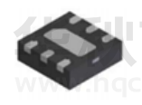
DFN2x2-6L
protection (OTP) function monitors chip temperature to
protect the device.
The WS3208D is available in DFN2x2-6L package.
Standard products are Pb-free and Halogen-free.
VIN 1
6
VIN 2
5 VOUT
GND 3
GND
VOUT
4 NC
Features
Pin configuration (Top view)
High voltage technology
Maximum input voltage
: 28V
Output power ON time
: 1.5ms (Typ.)
OVP threshold
: 5.7V (Typ.)
OVP response time
: 1us (Typ.)
OCP threshold
: 2A (Min.)
Output discharge
Package
:DFN2x2-6L
3208
= Device code
WD
= Company code
YW
= Year Week
Applications
GPS
PMP
MID
PAD
Digital cameras
Digital Videos
Will Semiconductor Ltd.
Marking
Order information
Device
WS3208D56-8/TR
1
Package
Shipping
DFN2x2-6L
3000/Reel&Tape
Aug, 2016 - Rev. 1.3
�WS3208D
Typical applications
Pin descriptions
Pin No.
Symbol
3
GND
WS3208
VIN
1,2
VIN
VOUT
VOUT
5,6
Descriptions
Power ground
Input pin, connect to AC
adaptor or VBUS. A 1uF low
1uF/50V
GND
3
ESR ceramic capacitor or
1uF
1,2
VIN
larger must be connected
as close as to this pin. It is
recommended to use 50V
capacitor or according to
application.
5,6
VOUT
Output pin, Connect to load.
Block diagram
OUT
IN
Charge Pump
OCP
Control
Logic
Vref
OTP
GND
Will Semiconductor Ltd.
2
Aug, 2016 - Rev. 1.3
�WS3208D
Absolute maximum ratings
Parameter
Input voltage (IN pin)
Output voltage (OUT pin)
Junction temperature
Lead temperature(10s)
Storage temperature
ESD Ratings
Symbol
Value
Unit
VIN
-0.3 ~ 28
V
VOUT
-0.3 ~ 6.5
V
150
o
260
o
Tstg
-55 ~ 150
o
HBM
±4000
V
MM
±400
V
TJ
TL
C
C
C
Recommend operating conditions (Ta=25oC, unless otherwise noted)
Parameter
Symbol
Value
Unit
Input voltage
VIN
3 ~ 28
V
Output current
IOUT
≤1.5
Ambient operating temperature
Will Semiconductor Ltd.
Topr
-40 ~ 85
3
A
o
C
Aug, 2016 - Rev. 1.3
�WS3208D
o
Electronics Characteristics (Ta=25 C, Vin=5V, Cin=Cout=1uF, unless otherwise noted)
Parameter
Symbol
Test conditions
Min.
Typ.
Max.
Unit
IOUT =0A
280
380
uA
IOUT =0.7A
190
250
mΩ
DC characteristics and Power-ON-Reset
Input quiescent current
IQ
IN-to-OUT ON resistance
RON
Output discharge resistance
RDISCHARGE
Under voltage lock out threshold
UVLO
VIN increasing from 0~3V
2.3
Under voltage lock out hysteresis
VHYS-UVLO
VIN decreasing from 3~0V
200
From Vin > UVLO to Vout =
0.9
Output power-on time
TON
Ω
500
2.9
V
250
300
mV
1.5
2.5
ms
90%×Voutset
Output power-on delay time
T1
From Vin > UVLO to Vout =
1.3
ms
0.2
ms
10%×Voutset
Output rise time
Tr
From Vout = 10%×Voutset to
Vout = 90%×Voutset
Input Over-Voltage-Protection (OVP)
OVP threshold
VOVP
VIN increasing from 5~7V
5.5
5.7
5.9
V
OVP hysteresis
VHYS-OVP
VIN decreasing from 7~5V
200
300
400
mV
OVP active time
TOVP
From Vin > VOVP to Vout began
1
us
to decline
OVP recovery time
TON(OVP)
From Vin < VOVP-VHYS-OVP to
0.9
1.5
2.5
ms
Vout = 90%×Voutset
Input Over-Current-Protection (OCP)
OCP threshold
IOCP
2.0
A
Over-Temperature-Protection (OTP)
OTP threshold
OTP hysteresis
165
o
40
o
C
TIMING DIAGRAMS
很抱歉,暂时无法提供与“WS3208D56-8/TR”相匹配的价格&库存,您可以联系我们找货
免费人工找货