SY8036
High Efficiency 5.5V, 6A, 1 MHz
Synchronous Step Down Regulator
General Description
Features
SY8036 is a high-efficiency 1 MHz synchronous stepdown DC-DC regulator IC capable of delivering up to
6A output current. SY8036 operates over a wide input
voltage range from 2.7V to 5.5V and integrates the
main switch and the synchronous switch with very low
RDS(ON) to minimize the conduction losses.
Low RDS(ON) for internal switches (top/bottom):
40/30mΩ
Input voltage range: 2.7-5.5V
1 MHz switching frequency minimizes the external
components
External adjustable softstart limits the inrush
current
100% dropout operation
Power good indicator
RoHS Compliant and Halogen Free
Compact package: DFN3x3-10
Low output voltage ripple and small external inductor
and capacitor sizes are achieved with 1MHz switching
frequency.
Ordering Information
SY8036□(□□)□
Applications
导
小
Package Type
DFN3×3-10
Note
6A
LCD TV
Access Point Router
Notebook PC
Server
l-F
or
半
Ordering Number
SY8036DBC
芯
Temperature Code
Package Code
Optional Spec Code
Sil
erg
yC
on
fid
C2
22µFх2
10
en
VIN: 2.7V to 5.5V
tia
Typical Applications
R6
10Ω
9
R4
100k
ON/ OFF
PVIN
LX
PVIN
LX
LX
8 SVIN
4
C7
1µF
1
5
GND
PG
EN
FB
SS
SY8036
L1 0.47µH
VOUT 1.8V
2
R2
100k
3
C4
C5
22pF 47µFх2
6
7
R1
50k
C8
(Opt.)
Figure 1: Typical application circuit diagram ( VOUT=1.8V)
SY8036 Rev.1.0
© 2018 Silergy Corp.
Silergy Corp. Confidential- Prepared for Customer Use Only
1
All Rights Reserved.
�SY8036
Pinout (top view)
LX 1
LX
2
LX
3
PG 4
EN 5
9 PVIN
11
GND
8 SVIN
7 SS
6 FB
Top Mark: CSxyz (device code: CS, x=year code, y=week code, z= lot number code)
Pin Number
Pin Description
PVIN
FB
9,10
6
PG
4
SS
7
Enable control. Pull high to turn on. Integrated 1M pull-down resistor.
Ground pin.
Phase node pin. Connect this pin to the inductor.
Signal power input pin. Decouple this pin to GND pin with at least 1µF
ceramic cap.
Power input pin. Decouple this pin to GND pin with at least 22µF ceramic cap.
Output feedback pin. Connect this pin to the center point of the output resistor
divider (as shown in Figure 1) to program the output voltage:
VOUT=0.6×(1+R1/R2).
Power good indicator(Open drain output). Low if the output < 90% of
regulation voltage; High otherwise. Connect a pull-up resistor to the input.
Softstart programming pin. Connect a capacitor from this pin to ground to
program the softstart time. Tss=Max(600us, Css×0.6V/10uA).
芯
5
11
1,2,3
8
半
EN
GND
LX
SVIN
导
小
Pin Name
10 PVIN
l-F
or
Absolute Maximum Ratings (Note 1)
Sil
erg
yC
on
fid
en
tia
Supply Input Voltage ---------------------------------------------------------------------------------------- -------- 0.3V to 6.5V
Enable, FB Voltage-------------------------------------------------------------------------------------------- 0.3V to VIN + 0.6V
Power Dissipation, PD @ TA = 25°C DFN3X3-10 ----------------------------------------------------------------------- 2.6W
Package Thermal Resistance (Note 2)
θ JA --------------------------------------------------------------------------------------------- ------------------ 38°C/W
θ JC ----------------------------------------------------------------------------------------------------------------- 8°C/W
Junction Temperature Range ------------------------------------------------------------------------------------ -40°C to 150°C
Lead Temperature (Soldering, 10 sec.) ------------------------------------------------------------------------------------ 260°C
Storage Temperature Range ------------------------------------------------------------------------------------- -65°C to 150°C
ESD Susceptibility (Note 2)
HBM (Human Body Mode) ---------------------------------------------------------------------------------------------------- 2kV
MM (Machine Mode) ------------------------------------------------------------------------------------- --------------------- 200V
Dynamic LX voltage in 50ns duration --------------------------------------------------------------------- IN+3V to GND-4V
Recommended Operating Conditions (Note 3)
Supply Input Voltage ----------------------------------------------------------------------------------------------- 2.7V to 5.5V
Junction Temperature Range ----------------------------------------------------------------------------------- -40°C to 125°C
Ambient Temperature Range ----------------------------------------------------------------------------------- -40°C to 85°C
SY8036 Rev.1.0
© 2018 Silergy Corp.
Silergy Corp. Confidential- Prepared for Customer Use Only
2
All Rights Reserved.
�SY8036
Electrical Characteristics
(VIN = 5V, VOUT = 2.5V, L = 0.47µH, COUT = 47µFх2, TA = 25°C, IOUT = 1A unless otherwise specified)
Parameter
Input Voltage Range
Shutdown Current
Quiescent Current
Feedback Reference
Voltage
FB Input Current
PFET RON
NFET RON
PFET Current Limit
EN Rising Threshold
EN Falling Threshold
Input UVLO Threshold
UVLO Hysteresis
Oscillator Frequency
Min ON Time
Max Duty Cycle
Thermal Shutdown
Temperature
Soft Start Time
Symbol
VIN
ISHDN
IQ
VREF
Test Conditions
IFB
RDS(ON)-P
RDS(ON)-N
ILIM
VENH
VENL
VUVLO
VHYS
FOSC
VFB=VIN
Min
2.7
EN=0
IOUT=0, VFB=VREF 105%
0.591
Typ
0.1
150
0.6
-50
50
7.5
1.5
0.4
2.7
0.2
1
80
IOUT=1A
Phase Node Discharge
Resistance
芯
Shutdown temperature
Hysteresis
CSS=100nF
Without CSS
导
小
tSS
0.609
40
30
100
TSD
Max
5.5
1
nA
mΩ
mΩ
A
V
V
V
V
MHz
ns
%
150
10
6
0.6
°C
ms
Ω
40
l-F
or
半
RDISCHG
Unit
V
µA
µA
V
fid
en
tia
Note 1: Stresses beyond the “Absolute Maximum Ratings” may cause permanent damage to the device. These are
stress ratings only. Functional operation of the device at these or any other conditions beyond those indicated in the
operational sections of the specification is not implied. Exposure to absolute maximum rating conditions for
extended periods may affect device reliability.
Sil
erg
yC
on
Note 2: ƟJA is measured in the natural convection at T A = 25°C on a low effective single layer thermal conductivity
test board of JEDEC 51-3 thermal measurement standard. Test condition: Device mounted on 2” x 2” FR-4 substrate
PCB, 2oz copper, with minimum recommended pad on top layer and thermal vias to bottom layer ground plane.
Note 3: The device is not guaranteed to function outside its operating conditions.
SY8036 Rev.1.0
© 2018 Silergy Corp.
Silergy Corp. Confidential- Prepared for Customer Use Only
3
All Rights Reserved.
�SY8036
DFN3x3-10 Package outline
PCB layout (recommended)
Side View
Sil
erg
yC
on
fid
en
tia
l-F
or
半
导
小
芯
Top View
Detail A
Pin1 identifier: two options
Bottom View
Notes: All dimensions are in millimeters and exclude mold flash & metal burr.
SY8036 Rev.1.0
© 2018 Silergy Corp.
Silergy Corp. Confidential- Prepared for Customer Use Only
4
All Rights Reserved.
�SY8036
Taping & Reel Specification
1. DFN3x3-10 taping orientation
3.9/4.1
11.7/12.3
1.45/1.55
芯
Feeding direction
导
小
2. Carrier Tape & Reel specification for packages
en
tia
l-F
or
半
Reel
Width
Sil
erg
yC
on
fid
Reel
Size
Package
types
Tape width
(mm)
Pocket
pitch(mm)
Reel size
(Inch)
Reel
width(mm)
Trailer
length(mm)
Leader length
(mm)
Qty per
reel
10
8
13"
12.4
400
400
5000
DFN3x3
3. Others: NA
SY8036 Rev.1.0
© 2018 Silergy Corp.
Powered by TCPDF (www.tcpdf.org)
Silergy Corp. Confidential- Prepared for Customer Use Only
5
All Rights Reserved.
�
很抱歉,暂时无法提供与“SY8036LDBC”相匹配的价格&库存,您可以联系我们找货
免费人工找货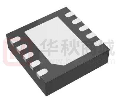


 工商网监
湘ICP备2023018690号
工商网监
湘ICP备2023018690号
