NSD1025
High Speed, 5A Dual-Channel,
Low-Side Gate Driver with Enable Pins
Datasheet (EN) 1.0
Product Overview
NSD1025 is a wide supply, non-inverting, dual-channel,
high speed, low side gate driver for both MOSFET, and
IGBT. It has capability to deliver 5A sink and source current
to the capacitive load along with rail-to-rail output to
reduce the Miller effect during MOSFET’s switching
transition. Fast rise and fall times as well as matched
propagation delay of both output channels enable the
NSD1025 suitable for high frequency power converter
application.
Both the input and enable pins of NSD1025 has ability to
handle -10V which enhance the noise immunity and
robustness of the device. Driver inputs are compatible
with CMOS and TTL logic hence it provides easy interface
with analog and digital controllers.
The internal circuitry provides an under voltage lockout
(UVLO) function by holding the output low until the supply
voltage is under the UVLO threshold values. Wide band of
VDD hysteresis between high and low thresholds offers
excellent noise immunity. The NSD1025 device is available
in SOP8, EP-SOP8, and EP-MSOP8 package with operating
temperature range from -40°C to 150°C.
Key Features
Wide supply voltage range: 4.5 to 24V
Source/Sink drive current: ±5A (Peak)
Two independent enable pins to control channel output
Short propagation delays: 21ns (typical)
Automotive qualified to AEC-Q100 Class 1
Applications
Typical SMPS (Solar, Server, Telecom, Industrial)
Motor Controllers
Pulse Transformer Driver
DC-DC Converters
Class-D switching amplifier
Line-drivers
Topologies
Synchronous rectifiers
Single and interleaved PFC
LLC
ZVS with pulsed transformer
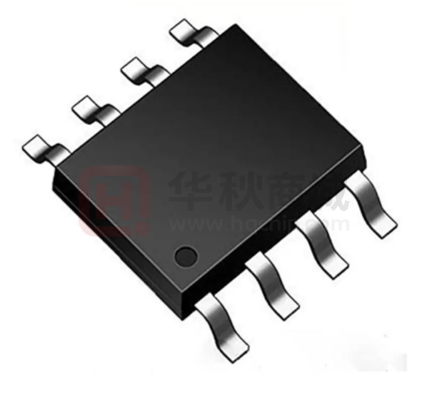
Device Information (1)
Part Number
NSD1025-DSPR
Package
SOP8
Body Size
4.9 mm × 3.9 mm
NSD1025-Q1HSPR
EP-SOP8
4.9 mm × 3.9 mm
NSD1025-Q1HMSR
EP-MSOP8
3.0 mm × 3.0 mm
NSD1025-DHMSR
EP-MSOP8
3.0 mm × 3.0 mm
1)
For all available packages, and order information refer to
the end of datasheet.
Block Diagram
Industry-standard Pin out
Ability to handle negative swing of (-10V) at each input pin
NSD1025
Offer High drive current by parallel connection of outputs
ENA
1
CMOS/TTL compatible logic inputs
INA
2
5A reverse current feature eliminates the need of output
protection circuitry
GND
3
INB
4
Operating temperature range: -40°C to 150°C
Low supply current
A
B
8
ENB
7
OUTA
6
VDD
5
OUTB
NSD1025 Block Diagram
Copyright © 2021, NOVOSENSE
Page 1
�NSD1025
Datasheet (EN) 1.0
INDEX
1. PIN CONFIGURATION AND FUNCTIONS ...................................................................................................................................... 3
2. ABSOLUTE MAXIMUM RATINGS ................................................................................................................................................. 4
3. RECOMMENDED OPERATING CONDITIONS ................................................................................................................................ 4
4. THERMAL INFORMATION ............................................................................................................................................................ 4
5. SPECIFICATIONS .......................................................................................................................................................................... 5
5.1
5.2
5.3
5.4
ELECTRICAL CHARACTERISTICS ................................................................................................................................................. 5
SWITCHING CHARACTERISTICS ................................................................................................................................................. 6
PARAMETERS MEASUREMENT INFORMATION ............................................................................................................................. 6
TYPICAL CHARACTERISTICS ...................................................................................................................................................... 7
6. DETAILED DESCRIPTION .............................................................................................................................................................. 9
6.1
6.2
6.3
OVERVIEW .......................................................................................................................................................................... 9
FUNCTIONAL BLOCK DIAGRAM .............................................................................................................................................. 10
FEATURE DESCRIPTION ......................................................................................................................................................... 10
6.3.1
6.3.2
6.3.3
6.3.4
6.3.5
Supply Voltage ........................................................................................................................................................................... 10
Under Voltage Lockout (UVLO) .................................................................................................................................................. 10
Input Stage ................................................................................................................................................................................. 11
Enable Function ......................................................................................................................................................................... 11
Device Functional Modes........................................................................................................................................................... 12
7. APPLICATIONS AND IMPLEMENTATION .................................................................................................................................... 13
7.1
7.2
7.3
TYPICAL APPLICATIONS......................................................................................................................................................... 13
DRIVER CURRENT AND POWER DISSIPATION ............................................................................................................................. 13
PCB LAYOUT...................................................................................................................................................................... 14
8. PACKAGE INFORMATION ........................................................................................................................................................... 15
9. ORDERING INFORMATION ........................................................................................................................................................ 16
10. DOCUMENTATION SUPPORT ................................................................................................................................................... 16
11. TAPE AND REEL INFORMATION ............................................................................................................................................... 17
12. REVISION HISTORY .................................................................................................................................................................. 19
Copyright © 2019, NOVOSENSE
Page 2
�NSD1025
Datasheet (EN) 1.0
1. Pin Configuration and Functions
NSD1025
14
ENA
ENB
8
2
INA
OUTA
7
3
GND
VDD
6
44
INB
OUTB
5
Figure. 1.1 NSD1025 Pin Configuration
Table 1.1 NSD1025 Pin Description
NSD1025
PIN NO.
SYMBOL
1
ENA
Channel A Enable Input: ENA is pulled up through a 180k resistor. if ENA is HIGH or left open OUTA
depends on INA; to disable the Channel A the ENA pin drive LOW regardless of the INA state
2
INA
Channel A Logic Input: INA is pulled down through a 180k resistor. OUTA is held LOW if INA is unbiased
or floating. This pin should be connected to HIGH state or GND (Not be left unconnected).
3
GND
Ground - Common ground reference for the device
4
INB
Channel B Logic Input: INB is pulled down through a 180k resistor. OUTB is held LOW if INB is unbiased
or floating. This pin should be connected to HIGH state or GND (Not be left unconnected).
5
OUTB
Channel B Output – Low impedance output with Source or sink current ability
6
VDD
Supply Voltage - Provides power to the device
7
OUTA
Channel A Output – Low impedance output with Source or sink current ability
8
ENB
FUNCTION
Channel B Enable Input: ENB is pulled up to VDD through a 180k resistor. if ENB is HIGH or left open
OUTB depends on INB; to disable the Channel B the ENB pin drive LOW regardless of the INB state
Copyright © 2021, NOVOSENSE
Page 3
�NSD1025
Datasheet (EN) 1.0
2. Absolute Maximum Ratings
Parameters
Supply Voltage
Input and Enable pins Voltage
Output Voltage
Symbol
Min
Max
Unit
Comments
VDD
-0.3
24
V
VINA, VINB, VENA, VENB
-10
24
V
-0.3
VDD+0.3
V
-2
VDD+0.3
V
Pulse
很抱歉,暂时无法提供与“NSD1025-DSPR”相匹配的价格&库存,您可以联系我们找货
免费人工找货