LM2577S/T-ADJ
General Description
The LM2577S/T-ADJ is a monolithic integrated circuit that provide all of
the power and control functions for step-up (boost), flyback, and forward
converter switching regulators.
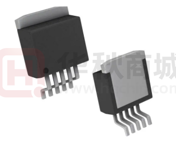
TO-220
Requiring a minimum number of external components, these regulators are
cost effective, and simple to use. Listed in this data sheet are a family of standard
inductors and flyback transformers designed to work with these switching
regulators.
TO-263
Included on the chip is a 3.0A NPN switch and its associated protection
circuitry, consisting of current and thermal limiting, and undervoltage lockout. Other features include a 52 kHz
fixed-frequency oscillator that requires no external components, a soft start mode to reduce in-rush current during
start-up, and current mode control for improved rejection of input voltage and output load transients.
The LM2577S is available in TO263-5L package.
The LM2577T is available in TO220-5L package.
Features
�
Requires few external components
�
NPN output switches 3.0A, can stand off 65V
�
Wide input voltage range: 3.5V to 40V
�
Current-mode operation for improved transient response, line regulation, and current limit
�
52 kHz internal oscillator
�
Soft-start function reduces in-rush current during start-up
�
Output switch protected by current limit, under-voltage lockout, and thermal shutdown
Applications
�
Simple boost regulator
�
Flyback and forward regulators
�
Multiple-output regulator
www.slkormicro.com
1
�LM2577S/T-ADJ
Pin Connection
Pin Description
LM2577S Absolute Maximum Ratings
If Military/Aerospace specified devices are required, please contact the National Semiconductor Sales
Office/Distributors for availability and specifications.
Characteristic
Limit
Unit
Supply voltage
45
V
Output switch voltage
65
V
6.0
A
Output switch current
*2
Power dissipation
Internally limited
-65~+150
℃
Lead temperature (soldering, 10 sec.)
260
℃
Maximum junction temperature
150
℃
2
kV
Storage temperature range
Minimum ESD rating (C=100pF, R=1.5kΩ)
Note 1: Absolute Maximum Ratings indicate limits beyond which damage to the device may occur. Operating
ratings indicate conditions the device is intended to be functional, but device parameter specifications may not be
guaranteed under these conditions. For guaranteed specifications and test conditions, see the Electrical
Characteristics.
Note 2: Due to timing considerations of the LM2577S/T_ADJ current limit circuit, output current cannot be
internally limited when the LM2577S/T_ADJ is used as a step-up regulator. To prevent damage to the switch,
its current must be externally limited to 6.0A. However, output current is internally limited when
the LM2577S/T_ADJ is used as a flyback or forward converter regulator in accordance to the Application Hints.
Recommended Operating Rating
Characteristic
Limit
Unit
3.5~40
V
Output switch voltage
0~60
V
Output switch current
≤3.0
A
-40~+125
℃
Supply voltage
Junction temperature range
www.slkormicro.com
2
�LM2577S/T-ADJ
Electrical Characteristics: (Specifications with standard type face are for TJ=25°C, and those in bold
type face apply over full Operating Temperature Range. Unless otherwise specified, VIN = 5V, and ISWITCH = 0.)
LM2577S/T_ADJ
VFEEDBACK=VREF
Characteristic
Symbol
System Parameters circuit of figure 3
Output voltage
VOUT
Line regulation
Load regulation
Efficiency
Device Parameters
Input supply current
Input supply undervoltage
lockout
Oscillator frequency
Output reference voltage
Output reference voltage
line regulator
Error amp input bias
current
Error amp
transconductance
η
IS
VUV
fO
VREF
Test conditions
*4
VIN=5V to 10V
ILOAD=100mA to 800mA *5
VIN=3.5V to 10V
ILOAD=300mA
VIN=5V,
ILOAD=100mA to 800mA
VIN=5V,ILOAD=800mA
Min.
*3
Typ.
Max
*3
Unit
11.60/
11.40
12
12.40/
12.60
V
20
50/
100
mV
20
50/
100
mV
80
VFEEDBACK=1.5V(switch off)
7.5
ISWITCH=2.0A
VCOMP=2.0V(max dutycycle)
25
ISWITCH=100mA
Measured at switch pin
ISWITCH=100mA
Measured at feedback pin
VIN=3.5V to 40V
VCOMP=1.0V
2.70/
2.65
48/
42
1.214/
1.206
2.90
52
1.230
%
10.0/
14.0
50/
85
3.10/
3.15
56/
62
1.246/
1.254
mA
mA
V
kHz
V
VIN=3.5V to 40V
0.5
mV
IB
VCOMP=1.0V
100
300/8
00
nA
GM
ICOMP=-30µ A to +30µ A
VCOMP=1.0V
2400/1
3700
5800
µ mho
500/
800
V/V
2.2/
2.0
2.4
V
Device Parameters
Error amp voltage gain
AVOL
Error amplifier output
swing
Error amplifier output
current
Soft start current
ISS
Maximum duty cycle
D
VCOMP=1.1V to 1.9V
RCOMP=1.0MΩ *6
Upper limit
VFEEDBACK=1.0V
Lower limit
VFEEDBACK=1.5V
VFEEDBACK=12.0V to 18.0V
VCOMP=1.0V
VFEEDBACK=1.0V
VCOMP=0V
VCOMP=1.5V
ISWITCH=100mA
Switch transconductance
www.slkormicro.com
3
0.3
0.40/
V
±130/
±200
±300/
µA
2.5/
1.5
5.0
7.5/
9.5
µA
93/
90
95
%
12.5
A/V
�LM2577S/T-ADJ
Switch leakage current
IL
Switch saturation current
VSAT
NPN switch current limit
VSWITCH=65V
VFEEDBACK=1.5V(switch off)
ISWITCH=2.0A
VCOMP=2.0V(max duty cycle)
VCOMP=2.0V
10
0.5
3.7/
3.0
4.3
Min.
Typ
300/
600
µA
0.7/
0.9
5.3/
6.0
V
A
Thermal Paramters (All Versions)
Characteristic
Thermal resistance
Symbol
θJA
θJC
θJA
Test conditions
TO-220, Junction to ambient
TO-220, Junction to case
TO-263, Junction to ambient
*7
65
2
Max
Unit
°C/W
37
*1: Absolute Maximum Ratings indicate limits beyond which damage to the device may occur. Operating ratings
indicate conditions the device is intended to be functional, but device parameter specifications may not be
guaranteed under these conditions. For guaranteed specifications and test conditions, see the Electrical
Characteristics.
*2: Due to timing considerations of the LM2577S/T_ADJ current limit circuit, output current cannot be internally
limited when the LM2577S/T_ADJ is used as a step-up regulator. To prevent damage to the switch, its
current must be externally limited to 6.0A. However, output current is internally limited when the LM2577S/T
_ADJ is used as a flyback or forward converter regulator in accordance to the Application Hints.
*3: All limits guaranteed at room temperature (standard type face) and at temperature extremes (boldface type).
All room temperature limits are 100% production tested. All limits at temperature extremes are guaranteed via
correlation using standard Statistical Quality Control (SQC) methods.
*4: External components such as the diode, inductor, input and output capacitors can affect switching regulator
performance. When the LM2577S/T_ADJ is used as shown in the Test Circuit, system performance will be as
specified by the system parameters.
*5: All limits guaranteed at room temperature (standard type face) and at temperature extremes (boldface type).
All limits are used to calculate Outgoing Quality Level, and are 100% production tested.
*6: A 1.0 MΩ resistor is connected to the compensation pin (which is the error amplifier’s output) to ensure
accuracy in measuring AVOL. In actual applications, this pin’s load resistance should be ≥10 MΩ, resulting in
AVOL that is typically twice the guaranteed minimum limit.
*7: If the TO-263 package is used, the thermal resistance can be reduced by increasing the PC board copper area
thermally connected to the package. Using 0.5 square inches of copper area, θJA is 50°C/W; with 1 square inch of
copper area, θJA is 37°C/W; and with 1.6 or more square inches of copper area, θJA is 32°C/W.
www.slkormicro.com
4
�LM2577S/T-ADJ
Test Circuit
FIGURE 3. Circuit Used to Specify System Parameters for ADJ Versions
L = 415-0930 (AIE)
D = any manufacturer
COUT = Sprague Type 673D
Electrolytic 680 µF, 20V
R1 = 48.7k in series with 511Ω (1%)
www.slkormicro.com
5
R2 = 5.62k (1%)
�LM2577S/T-ADJ
D2577-ADJ
FIGURE 4. LM2577S/T_ADJ Block Diagram and Boost Regulator Application
Step-Up (boost) Regulator
Figure 4 shows the LM2577S/T_ADJ-ADJ used as a Step-Up Regulator. This is a switching regulator used
for producing an output voltage greater than the input supply voltage. The LM2577S/T_ADJ-12
and LM2577S/T_ADJ-15 can also be used for step-up regulators with 12V or 15V outputs (respectively), by
tying the feedback pin directly to the regulator output.
A basic explanation of how it works is as follows. The LM2577S/T_ADJ turns its output switch on and off at
a frequency of 52 kHz, and this creates energy in the inductor (L). When the NPN switch turns on, the inductor
current charges up at a rate of VIN/L, storing current in the inductor.When the switch turns off, the lower end of
www.slkormicro.com
6
�LM2577S/T-ADJ
the inductor flies above VIN, discharging its current through diode (D) into the output capacitor (COUT) at a rate of
(VOUT − VIN)/L. Thus, energy stored in the inductor during the switch on time is transferred to the output during
the switch off time. The output voltage is controlled by the amount of energy transferred which, in turn, is
controlled by modulating the peak inductor current. This is done by feeding back a portion of the output voltage to
the error amp,
which amplifies the difference between the feedback voltage and a 1.230V reference.The error amp output
voltage is compared to a voltage proportional to the switch current (i.e., inductor current during the switch on
time).
The comparator terminates the switch on time when the two voltages are equal, thereby controlling the peak
switch current to maintain a constant output voltage. Voltage and current waveforms for this circuit are shown in
Figure 5, and formulas for calculating them are given in Figure 6.
FIGURE 5. Step-Up Regulator Waveforms
FIGURE 6. Step-Up Regulator Formulas
Step-Up Regulator Design Procedure
The following design procedure can be used to select the appropriate external components for the circuit in
www.slkormicro.com
7
�LM2577S/T-ADJ
Figure 4, based on these system requirements.
Given:
VIN (min) = Minimum input supply voltage
VOUT = Regulated output voltage
ILOAD(max) = Maximum output load current
Before proceeding any further, determine if the LM2577S/T_ADJ can provide these values of VOUT and
ILOAD(max) when operating with the minimum value of VIN. The upper limits for VOUT and ILOAD(max) are given
by the following equations.
VOUT ≤ 60V
and VOUT ≤ 10 x VIN(min)
These limits must be greater than or equal to the values specified in this application.
1. Inductor Selection (L)
A. Voltage Options:
1. For 12V or 15V output From Figure 7 (for 12V output) or Figure 8 (for 15V output), identify inductor code for
region indicated by VIN
(min)
and ILOAD
(max).
The shaded region indicates conditions for which the
LM2577S/T_ADJ output switch would be operating beyond its switch current rating. The minimum operating
voltage for the LM2577S/T_ADJ is 3.5V. From here, proceed to step C.
2. For Adjustable version Preliminary calculations:
The inductor selection is based on the calculation of the following three parameters:
D(max), the maximum switch duty cycle (0 ≤ D ≤ 0.9):
where VF = 0.5V for Schottky diodes and 0.8V for fast recovery diodes (typically);
E •T, the product of volts x time that charges the inductor:
IIND,DC, the average inductor current under full load;
B. Identify Inductor Value:
1. From Figure 9, identify the inductor code for the region indicated by the intersection of E•T and IIND,DC.This
www.slkormicro.com
8
�LM2577S/T-ADJ
code gives the inductor value in microhenries. The L or H prefix signifies whether the inductor is rated for a
maximum E•T of 90 V•µs (L) or 250 V•µs (H).
2. If D < 0.85, go on to step C. If D ≥ 0.85, then calculate the minimum inductance needed to ensure the switching
regulator’s stability:
If LMIN is smaller than the inductor value found in step B1, go on to step C. Otherwise, the inductor value
found in step B1 is too low; an appropriate inductor code should be obtained from the graph as follows:
1. Find the lowest value inductor that is greater than LMIN.
2. Find where E•T intersects this inductor value to determine if it has an L or H prefix. If E•T intersects both the L
and H regions, select the inductor with an H prefix.
FIGURE 7. LM2577S/T_ADJ-12 Inductor Selection Guide
Inductor Selection Guide
www.slkormicro.com
9
FIGURE 8.LM2577S/T_ADJ-15
�LM2577S/T-ADJ
Note: These charts assume that
the
inductor
ripple
current
inductor is approximately 20% to
30% of the average inductor
current (when the regulator is
under full load). Greater ripple
current causes higher peak switch
currents and greater output ripple
voltage; lower ripple current is
achieved
with
larger-value
inductors. The factor of 20 to
30% is chosen as a convenient
balance
between
the
two
FIGURE 9. LM2577S/T_ADJ-ADJ Inductor Selection Graph
C. Select an inductor from the table of Figure 10 which cross-references the inductor codes to the part numbers of
three different manufacturers. Complete specifications for these inductors are available from the respective
manufacturers. The inductors listed in this table have the following characteristics:
AIE: ferrite, pot-core inductors; Benefits of this type are low electro-magnetic interference (EMI), small physical
size, and very low power dissipation (core loss). Be careful not to operate these inductors too far beyond their
maximum ratings for E•T and peak current, as this will saturate the core.
Pulse: powdered iron, toroid core inductors; Benefits are low EMI and ability to withstand E•T and peak current
above rated value better than ferrite cores.
Renco: ferrite, bobbin-core inductors; Benefits are low cost and best ability to withstand E•T and peak current
above rated value. Be aware that these inductors generate more EMI than the other types, and this may interfere
with signals sensitive to noise.
www.slkormicro.com
10
�LM2577S/T-ADJ
FIGURE 10. Table of Standardized Inductors and Manufacturer’s Part Numbers
2. Compensation Network (RC, CC) and Output Capacitor(COUT) Selection
RC and CC form a pole-zero compensation network that stabilizes the regulator. The values of RC and CC are
mainly dependant on the regulator voltage gain, ILOAD(max), L and COUT. The following procedure calculates
values for RC, CC, and COUT that ensure regulator stability. Be aware that this procedure doesn’t necessarily result
in RC and CC that provide optimum compensation. In order to guarantee optimum compensation, one of the
standard procedures for testing loop stability must be used, such as measuring VOUT transient response when
pulsing ILOAD (see Figure 15).
A. First, calculate the maximum value for RC.
Select a resistor less than or equal to this value, and it should also be no greater than 3 kΩ.
B. Calculate the minimum value for COUT using the following two equations.
www.slkormicro.com
11
�LM2577S/T-ADJ
The larger of these two values is the minimum value that ensures stability.
C. Calculate the minimum value of CC .
The compensation capacitor is also part of the soft start circuitry. When power to the regulator is turned on,
the switch duty cycle is allowed to rise at a rate controlled by this capacitor (with no control on the duty cycle, it
would immediately rise to 90%, drawing huge currents from the input power supply). In order to operate properly,
the soft start circuit requires CC ≥ 0.22 µF.
The value of the output filter capacitor is normally large enough to require the use of aluminum electrolytic
capacitors. Figure 11 lists several different types that are recommended for switching regulators, and the
following parameters are used to select the proper capacitor.
Working Voltage (WVDC): Choose a capacitor with a working voltage at least 20% higher than the regulator
output voltage.
Ripple Current: This is the maximum RMS value of current that charges the capacitor during each switching cycle.
For step-up and flyback regulators, the formula for ripple current is
Choose a capacitor that is rated at least 50% higher than this value at 52 kHz.
Equivalent Series Resistance (ESR) : This is the primary cause of output ripple voltage, and it also affects the
values of RC and CC needed to stabilize the regulator. As a result, the preceding calculations for CC and RC are
only valid if ESR doesn’t exceed the maximum value specified by the following equations.
Select a capacitor with ESR, at 52 kHz, that is less than or equal to the lower value calculated. Most
electrolytic capacitors specify ESR at 120 Hz which is 15% to 30% higher than at 52 kHz. Also, be aware that
ESR increases by a factor of 2 when operating at −20°C.
In general, low values of ESR are achieved by using large value capacitors (C ≥ 470 µF), and capacitors with
high WVDC, or by paralleling smaller-value capacitors.
3. Output Voltage Selection (R1 and R2)
This section is for applications using the LM2577S/T_ADJ-ADJ. Skip this section if the LM2577S/T_ADJ12 or LM2577S/T_ADJ-15 is being
www.slkormicro.com
12
�LM2577S/T-ADJ
used. With the LM2577S/T_ADJ-ADJ, the output voltage is given by
VOUT = 1.23V (1 + R1/R2)
Resistors R1 and R2 divide the output down so it can be compared with the LM2577S/T_ADJ-ADJ internal
1.23V reference. For a given desired output voltage VOUT, select R1 and R2 so that
4. Diode Selection (D)
The switching diode used in the boost regulator must withstand a reverse voltage equal to the circuit output
voltage,and must conduct the peak output current of the LM2577S/T_ADJ. A suitable diode must have a minimum
reverse breakdown voltage greater than the circuit output voltage, and should be rated for average and peak
current greater than ILOAD(max) and ID(PK). Schottky barrier diodes are often favored for use in switching
regulators. Their low forward voltage drop allows higher regulator efficiency than if a (less expensive) fast
recovery diode was used. See Figure 11 for recommended part numbers and voltage ratings of 1A and 3A diodes.
FIGURE 11. Diode Selection Chart
www.slkormicro.com
13
�LM2577S/T-ADJ
Flyback Regulator Design Procedure
1. Transformer Selection
A family of standardized flyback transformers is available for creating flyback regulators that produce dual
output voltages, from ±10V to ±15V, as shown in Figure 17. Figure 19 lists these transformers with the input
voltage, output voltages and maximum load current they are designed for.
T1 = Pulse Engineering, PE-65300
D1, D2 = 1N5821
FIGURE 17. LM2577S/T_ADJ-ADJ Flyback Regulator with ± Outputs
www.slkormicro.com
14
�LM2577S/T-ADJ
FIGURE 18. Flyback Regulator Formulas
C. Calculate the minimum value of CC
D. Calculate the maximum ESR of the +VOUT and −VOUT output capacitors in parallel.
This formula can also be used to calculate the maximum ESR of a single output regulator.
At this point, refer to this same section in the Step-Up Regulator Design Procedure for more information
regarding the selection of COUT.
www.slkormicro.com
15
�LM2577S/T-ADJ
3. Output Voltage Selection
This section is for applications using the LM2577S/T_ADJ-ADJ. Skip this section if the LM2577S/T_ADJ12 or LM2577S/T_ADJ-15 is being used.With the LM2577S/T_ADJ-ADJ, the output voltage isgiven by
VOUT = 1.23V (1 + R1/R2)
Resistors R1 and R2 divide the output voltage down so it can be compared with the LM2577S/T_ADJ-ADJ
internal 1.23V reference. For a desired output voltage VOUT, select R1 and R2 so that
4. Diode Selection
The switching diode in a flyback converter must withstand the reverse voltage specified by the following
equation.
A suitable diode must have a reverse voltage rating greater than this. In addition it must be rated for more
than the average and peak diode currents listed in Figure 18.
5. Input Capacitor Selection
The primary of a flyback transformer draws discontinuous pulses of current from the input supply. As a
result, a flyback regulator generates more noise at the input supply than a step-up regulator, and this requires a
larger bypass capacitor to decouple the LM2577S/T_ADJ VIN pin from this noise. For most applications, a low
ESR, 1.0 µF cap will be sufficient, if it is connected very close to the VIN and Ground pins.
www.slkormicro.com
16
�LM2577S/T-ADJ
FIGURE 19. Flyback Transformer
Selection Guide
In addition to this bypass cap, a larger capacitor (≥ 47 µF) should be used where the flyback transformer
connects to the input supply. This will attenuate noise which may interfere with other circuits connected to the
same input supply voltage.
www.slkormicro.com
17
�LM2577S/T-ADJ
Outline Drawing
TO-220
Unit:mm
TO-263
Unit: mm
www.slkormicro.com
18
�