TP485E
±18K ESD Protection, Bus-Polarity Correcting RS-485 Transceiver
Features
Description
Exceeds Requirements of EIA-485 Standard
The TP485E is a low-power RS-485 transceiver with
Bus-Polarity Correction within 100 ms (tFS)
automatic bus-polarity
Data Rate: 300 bps to 250 kbps
Works with Two Configurations:
correction
and
transient
protection. Upon hot plug-in, the device detects and
corrects the bus polarity within the first 100 ms of bus
idling. On-chip transient protection protects the device
– Failsafe Resistors Only
against IEC61000 ESD and EFT transients. This device
– Failsafe and Differential Termination Resistors
has robust
Up to 256 Nodes on a Bus (1/8 unit load)
industrial applications. The bus pins are robust to
Wide Supply Voltage 3V to 5.5V
electrostatic discharge (ESD) events, with high levels of
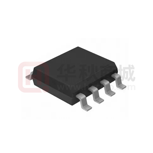
SOIC-8 Package for Backward Compatibility
protection
Bus-Pin Protection:
drivers
to
and receivers
Human-Body
for demanding
Model (HBM),
Air-Gap
Discharge, and Contact Discharge specifications. The
device combines a differential driver and a differential
– ±18 kV HBM protection
receiver, which operate together from a single 5-V power
– ±13 kV IEC61000-4-2 Contact Discharge
supply.
– +4 kV IEC61000-4-4 Fast Transient Burst
differential inputs are connected internally to form a bus
Applications
The driver differential outputs and the receiver
port suitable for half-duplex(two-wire bus) communication.
The device features a wide common-mode voltage range
E-Metering Networks
making the device suitable for multi-point applications
Industrial Automation
over long cable runs. The TP485E is available in both
HVAC Systems
SOIC-8 and MSOP-8 package, and is characterized from
Process Control
–40°C to 125°C.
DMX512-Networks
Battery-Powered Applications
3PEAK and the 3PEAK logo are registered trademarks of
3PEAK INCORPORATED. All other trademarks are the property of
their respective owners.
Pin Configuration (Top View)
TP485E
8-Pin SOIC/MSOP
-S and -V Suffixes
R
VCC
RE
B/Z
DE
A/Y
D
www.3peakic.com
GND
Rev.A
1
�TP485E
±18K ESD Protection, Bus-Polarity Correcting RS-485 Transceiver
Order Information
Model Name
Order Number
Package
Transport Media, Quantity
Marking
Information
TP485E
TP485E-SR
8-Pin SOIC
Tape and Reel, 4,000
TP485E
TP485E
TP485E-VR
8-Pin MSOP
Tape and Reel, 3,000
TP485E
DRIVER PIN FUNCTIONS
INPUT
ENABLE
D
DE
OUTPUTS
A
DESCRIPTION
B
NORMAL MODE
H
H
H
L
Actively drives bus High
L
H
L
H
Actively drives bus Low
X
L
Z
Z
Driver disabled
X
OPEN
Z
Z
Driver disabled by default
OPEN
H
H
L
Actively drives bus High
POLARITY-CORRECTING MODE (1)
H
H
L
H
Actively drives bus Low
L
H
H
L
Actively drives bus High
X
L
Z
Z
Driver disabled
X
OPEN
Z
Z
Driver disabled by default
OPEN
H
L
H
Actively drives bus Low
(1)
The polarity-correcting mode is entered when VID < VIT– and t > tFS and DE = low. This state is latched when /RE turns from Low to
High.
RECEIVER PIN FUNCTIONS
DIFFERENTIAL
INPUT
VID = VA – VB
ENABLE
OUTPUT
/RE
R
DESCRIPTION
NORMAL MODE
VIT+ < VID
L
H
Receive valid bus High
VIT– < VID < VIT+
L
?
Indeterminate bus state
VID < VIT–
L
L
Receive valid bus Low
X
H
Z
Receiver disabled
X
OPEN
Z
Receiver disabled
Open, short, idle Bus
L
?
Indeterminate bus state
POLARITY-CORRECTING MODE (1)
VIT+ < VID
L
L
Receive valid bus Low
VIT– < VID < VIT+
L
?
Indeterminate bus state
VID < VIT–
L
H
Receive polarity corrected bus High
X
H
Z
Receiver disabled
X
OPEN
Z
Receiver disabled
Open, short, idle Bus
L
?
Indeterminate bus state
(1)
2
The polarity-correcting mode is entered when VID < VIT– and t > tFS and DE = low. This state is latched when /RE turns from Low to
High.
Rev.A
www.3peakic.com
�
TP485E
±18K ESD Protection, Bus-Polarity Correcting RS-485 Transceiver
Absolute Maximum Ratings
VDD to GND.........................................................................................................................................-0.3V to +7V
Input Voltages
DI, DE, RE………………………………………………………………………….……………………….....-0.3V to (VCC + 0.3V)
Input/Output Voltages
A/Y, B/Z, A, B, Y, Z………………………………………………………………………..……….…….…...-15V to +15V
A/Y, B/Z, A, B, Y, Z (Transient Pulse Through 100Ω,
Note 1)………………………………………………………………………………………….……….….… ±100V
RO……………………………………………………………………………………………………….……. -0.3V to (VCC +0.3V)
Short Circuit Duration
Y, Z…………………………………………………………………………………………………………..….Continuous
ESD Rating………………………………………………………………………………………………..……See Specification Table
Recommended Operating Conditions
Note 2
Supply Voltage………………………………………………………………………………….………..…….3V to 5.5V
Temperature Range……………………………………………………………………………………...……-40°C to +125°C
Bus Pin Common Mode Voltage Range ……………………………………………………………..……..-8V to +13V
Thermal Resistance, ΘJA (Typical)
8-Pin SOIC Package ……………………………………………………………….…………………...……158°C/W
8-Pin MSOP Package ……………………………………………………………….……………………..…210°C/W
Maximum Junction Temperature (Plastic Package) …………………………………………...………….+150°C
Maximum Storage Temperature Range ………………………………………………………..…………. -65°C to +150°C
Note 1: Tested according to TIA/EIA-485-A, Section 4.2.6 (±100V for 15μs at a 1% duty cycle).
Note 2: Do not operate at or near the maximum ratings listed for extended periods of time. Exposure to such conditions may adversely impact
product reliability and result in failures not covered by warranty.
www.3peakic.com
Rev.A
3
�TP485E
±18K ESD Protection, Bus-Polarity Correcting RS-485 Transceiver
Electrical Characteristics
Test Conditions: VCC = 5V, Over operating free-air temperature range(unless otherwise noted)
PARAMETER
CONDITIONS
RL = 60 Ω
MIN
See Figure 1B
TYP
MAX
UNITS
2.6
RL = 54 Ω with VA or
VB from –7 to +12 V,
|VOD|
Driver differential-output voltage
VCC = 5V (RS-485)
magnitude
RL = 54 Ω with VA or
2.4
2.6
V
See Figure 1A
VB from -7 to +12 V,
1.4
1.5
VCC = 3V (RS-485)
RL = 100 Ω(RS-422)
⊿|VOD|
VOC(SS)
⊿VOC
VOC(PP)
COD
Change in magnitude of driver
differential-output voltage
RL = 54 Ω, CL=50pF
3
See Figure 1A
-0.01
Vcc/2-
Steady-stage common-mode
output voltage
Change in differential driver
0.2
Center of two 27-Ω
common-mode output voltage
load resistors
See Figure 1A
-0.2
Peak-to-peak driver
Positive-going receiver
differential-input voltage threshold
Negative-going receiver
VIT-
differential-input voltage threshold
(1)
VHYS
VCC/2
0
0.03
Vcc/2
+0.2
0.2
V
V
mV
500
common-mode output voltage
Differential output capacitance
VIT+
0
Receiver differential-input voltage
threshold hysteresis (VIT+ – VIT– )
8
pF
75
mV
-75
mV
150
mV
VOH
Receiver high-level output voltage
IOH= -8 mA
4.64
4.65
4.66
V
VOL
Receiver low-level output voltage
IOL= 8 mA
0.22
0.23
0.24
V
0.012
0.017
0.022
μA
-0.003
0
0.01
μA
80
107
mA
55
65
II
IOZ
Driver input, driver enable and
receiver enable input current
Receiver high-impedance output
current
|IOS|
Driver short-circuit output current
II
Bus input current(driver disabled)
VO = 0 V or VCC, /RE at VCC
│IOS│ with VA or VB from –7 to +12 V
VCC = 4.5 to 5.5 V or
VI= 12 V
VCC = 0 V, DE at 0 V
VI= -7 V
Driver and receiver
enabled
Driver enabled,
receiver disabled
ICC
Supply current(quiescent)
Driver disabled,
receiver enabled
Driver and receiver
disabled
Supply current(dynamic)
4
Rev.A
DE
=
-63
-50
624
680
771
269
278
290
458
500
546
0.017
0.15
0.177
μA
VCC,
/RE = GND,
No LOAD
DE
=
VCC,
/RE = VCC, No
LOAD
μA
DE = GND,
/RE = VCC, No
LOAD
DE = GND,
/RE = VCC, D=
Vcc No LOAD
See
www.3peakic.com
�
TP485E
±18K ESD Protection, Bus-Polarity Correcting RS-485 Transceiver
Switching CHARACTERISTICS
.3.3ms > bit time> 4μs(unless otherwise noted)
PARAMETER
CONDITIONS
MIN
TYP
MAX
UNITS
DRIVER
tr, tf
Driver differential-output rise and
620
fall times
RL = 54 Ω, CL=50pF
340
See Figure 2
tPHL, tPLH
Driver propagation delay
tSK(P)
Driver pulse skew, |tPHL – tPLH|
23
tPHZ, tPLZ
Driver disable time
250
tPHZ, tPLZ
Driver enable time
Receiver enabled
See Figure 3
ns
ns
562
Receiver disabled
ns
562
RECEIVER
tr, tf
Receiver output rise and fall times
tPHL, tPLH
Receiver propagation delay time
tSK(P)
Receiver pulse skew, |tPHL – tPLH|
40
tPHZ, tPLZ
Receiver disable time
7
tPZL(1),
tPZH(1)
12.4
CL=15 pF
960
See Figure 5
ns
ns
Driver enabled
See Figure 6
70
Driver disabled
See Figure 6
989
Driver disabled
See Figure 6
Receiver enable time
tPZL(2),
ns
tPZH(2)
tFS
Bus failsafe time
www.3peakic.com
88
100
Rev.A
107
ms
5
�TP485E
±18K ESD Protection, Bus-Polarity Correcting RS-485 Transceiver
Test Circuits and Waveforms
FIGURE 1A. VOD AND VOC
FIGURE 1B. VOD WITH COMMON MODE LOAD
FIGURE 1. DC DRIVER TEST CIRCUITS
FIGURE 2A. TEST CIRCUIT
FIGURE 2B. MEASUREMENT POINTS
FIGURE 2. DRIVER PROPAGATION DELAY AND DIFFERENTIAL TRANSITION TIMES
PARAMETER
OUTPUT
RE
DI
DE
3V
NOTE 10
CL
tZH,tZH(SHDN)
(pF)
NOTE 10
SW
OUT(Y,Z)
tHZ
Y/Z
X
1/0
GND
15
tLZ
Y/Z
X
0/1
VCC
15
tZL,tZL(SHDN)
tZH
Y/Z
0 (Note 9)
1/0
GND
100
NOTE 10
tZL
Y/Z
0 (Note 9)
0/1
VCC
100
tZH(SHDN)
Y/Z
1 (Note 12)
1/0
GND
100
tZL(SHDN)
Y/Z
1 (Note 12)
0/1
VCC
100
FIGURE 3A. TEST CIRCUIT
OUT(Y,Z)
1.5V
1.5V
0V
tHZ
OUTPUT HIGH
2.3V
VOL-0.5V VOH
0V
tLZ
2.3V
VCC
VOL+0.5V VOL
OUTPUT LOW
FIGURE 3B. MEASUREMENT POINTS
FIGURE 3. DRIVER ENABLE AND DISABLE TIMES
6
Rev.A
www.3peakic.com
�
TP485E
±18K ESD Protection, Bus-Polarity Correcting RS-485 Transceiver
Test Circuits and Waveforms(continue)
FIGURE 4A. TEST CIRCUIT
FIGURE 4B. MEASUREMENT POINTS
FIGURE 4. DRIVER DATA RATE
FIGURE 5A. TEST CIRCUIT
FIGURE 5B. MEASUREMENT POINTS
FIGURE 5. RECEIVER PROPAGATION DELAY AND DATA RATE
NOTE 10
PARAMETER
DE
tHZ
0
A
+1.5V
SW
RE
tZH,tZH(SHDN)
GND
NOTE 10
RO
tLZ
0
-1.5V
VCC
tZH(Note 10)
0
+1.5V
GND
tZL,tZL(SHDN)
tZL(Note 10)
0
-1.5V
VCC
NOTE 10
tZH(SHDN)(Note 13)
tZL(SHDN)(Note 13)
0
0
+1.5V
-1.5V
GND
VCC
RO
3V
1.5V
1.5V
0V
tHZ
OUTPUT HIGH
1.5V
VOH-0.5V VOH
0V
tLZ
1.5V
VCC
VOL+0.5V VOL
OUTPUT LOW
FIGURE 6A. TEST CIRCUIT
FIGURE 6B. MEASUREMENT POINTS
FIGURE 6. RECEIVER ENABLE AND DISABLE TIMES
www.3peakic.com
Rev.A
7
�TP485E
±18K ESD Protection, Bus-Polarity Correcting RS-485 Transceiver
Detailed Description
The TP485E half-duplex RS-485 transceiver features automatic polarity correction on the RS-485 bus lines. This device also
includes fail-safe circuitry, which guarantees a logic-high receiver output when the receiver inputs are open or shorted, or
when connected to a terminated transmission line with all drivers disabled. Hot-swap capability on the enable inputs allows
line insertion without erroneous data transfer and controlled slew-rate drivers minimize EMI and reduce reflections caused by
improperly terminated cables, allowing error-free data transmission up to 250 kbps. The TP485E features short-circuit current
limits on the driver and receiver outputs and thermal shutdown circuitry to protect against excessive power dissipation.
Automatic Polarity Detection
The TP485E is designed to detect and correct installation-based connections on RS-485 lines. With the driver disabled,
internal detection circuitry samples the voltages at the A and B inputs during an idle period (100ms, typ) and configures the
driver and receiver for the detected polarity. Polarity is swapped only when |VA – VB| > 75mV for the idle period. The A/B line
polarity can be defined by a pull up and pull down resistor pair on the A/B lines, for example, in the RS-485 Half duplex
master terminal (see the Typical Operating Circuit). When the polarity is normal, A is the non inverting receiver input/driver
output and B is the inverting input/output. When the polarity is inverted, A is the inverting input/output and B is the non
inverting input/output.
To allow the bus to define A/B polarity, connect one pull up/pull down resistor pair to the bus to set the bus status during the
idle periods. It is preferable to locate the resistor pair in the bus master, as shown in Figure 7.
Figure 7. Polarity Definition
Hot Plug Function
When a piece of equipment powers up, there is a period of time where the processor or ASIC driving the RS-485 control lines (DE,
RE) is unable to ensure that the RS-485 Tx and Rx outputs are kept disabled. If the equipment is connected to the bus, a driver
activating prematurely during power-up may crash the bus. To avoid this scenario, the TP485E devices incorporate a “Hot Plug”
function. Circuitry monitoring VCC ensures that, during power-up and power-down, the Tx and Rx outputs remain disabled,
regardless of the state of DE and RE, if VCC is less than ~2.5V. This gives the processor/ASIC a chance to stabilize and drive the
RS-485 control lines to the proper states.
8
Rev.A
www.3peakic.com
�
TP485E
±18K ESD Protection, Bus-Polarity Correcting RS-485 Transceiver
FIGURE 8. HOT PLUG PERFORMANCE (TP485E) vs Competitor WITHOUT HOT PLUG CIRCUITRY
ESD Protection
All pins on these devices include class 3 (>7 kV) Human Body Model (HBM) ESD protection structures, but the RS-485 pins (driver
outputs and receiver inputs) incorporate advanced structures allowing them to survive ESD events in excess of ±18 kV HBM and
±13 kV (1/2 duplex) IEC61000-4-2. The RS-485 pins are particularly vulnerable to ESD strikes because they typically connect to an
exposed port on the exterior of the finished product. Simply touching the port pins, or connecting a cable, can cause an ESD event
that might destroy unprotected ICs. These new ESD structures protect the device whether or not it is powered up, and without
degrading the RS-485 common mode range of -7V to +12V. This built-in ESD protection eliminates the need for board level
protection structures (e.g., transient suppression diodes), and the associated, undesirable capacitive load they present.
Transient Protection
The bus terminals of the TP485E transceiver family possess on-chip ESD protection against ±18 kV HBM and ±13 kV IEC61000-4-2
contact discharge. The International Electrotechnical Commision (IEC) ESD test is far more severe than the HBM ESD test. The
50% higher charge capacitance, CS, and 78% lower discharge resistance, RD of the IEC model produce significantly higher
discharge currents than the HBM model.
As stated in the IEC 61000-4-2 standard, contact discharge is the preferred transient protection test method. Although IEC air-gap
testing is less repeatable than contact testing, air discharge protection levels are inferred from the contact discharge test results.
www.3peakic.com
Rev.A
9
�TP485E
±18K ESD Protection, Bus-Polarity Correcting RS-485 Transceiver
Figure 9.
HBM and IEC-ESD Models and Currents in Comparison (HBM Values in Parenthesis)
The on-chip implementation of IEC ESD protection significantly increases the robustness of equipment. Common discharge events
occur because of human contact with connectors and cables. Designers may choose to implement protection against longer
duration transients, typically referred to as surge transients. Figure 9 suggests two circuit designs providing protection against short
and long duration surge transients, in addition to ESD and Electrical Fast Transients (EFT) transients. Table 1 lists the bill of
materials for the external protection devices.
EFTs are generally caused by relay-contact bounce or the interruption of inductive loads. Surge transients often result from lightning
strikes (direct strike or an indirect strike which induce voltages and currents), or the switching of power systems, including load
changes and short circuits switching. These transients are often encountered in industrial environments, such as factory automation
and power-grid systems. Figure 10 compares the pulse-power of the EFT and surge transients with the power caused by an IEC
ESD transient. In the diagram on the left of Figure 10, the tiny blue blip in the bottom left corner represents the power of a 10-kV ESD
transient, which already dwarfs against the significantly higher EFT power spike, and certainly dwarfs against the 500-V surge
transient. This type of transient power is well representative of factory environments in industrial and process automation. The
diagram on the fright of Figure 10 compares the enormous power of a 6-kV surge transient, most likely occurring in e-metering
applications of power generating and power grid systems, with the aforementioned 500-V surge transient.
Figure 10. Power Comparison of ESD, EFT, and Surge Transients
In the case of surge transients, high-energy content is signified by long pulse duration and slow decaying pulse Power The electrical
energy of a transient that is dumped into the internal protection cells of the transceiver is converted into thermal energy. This thermal
10
Rev.A
www.3peakic.com
�
TP485E
±18K ESD Protection, Bus-Polarity Correcting RS-485 Transceiver
energy heats the protection cells and literally destroys them, thus destroying the transceiver. Figure 11 shows the large differences
in transient energies for single ESD, EFT, and surge transients as well as for an EFT pulse train, commonly applied during
compliance testing.
Figure 11. Comparison of Transient Energies
Table 1. Bill of Materials
Device
Function
Order Number
Manufacturer
485
5-V, 250-kbps RS-485 Transceiver
TP485E
R1, R2
10-Ω, Pulse-Proof Thick-Film Resistor
CRCW0603010RJNEAHP
TVS
Bidirectional 400-W Transient Suppressor
CDSOT23-SM712
Bourns
TBU1, TBU2
Bidirectional.
200mA Transient Blocking Unit 200-V, MetalOxide Varistor
TBU-CA-065-200-WH
Bourns
MOV1, MOV2
Figure 12.
3PEAK
Vishay
MOV-10D201K
Bourns
Transient Protections Against ESD, EFT, and Surge Transients
The left circuit shown in Figure 12 provides surge protection of ≥ 500-V transients, while the right protection circuits can
withstand surge transients of 5 kV.
www.3peakic.com
Rev.A
11
�TP485E
±18K ESD Protection, Bus-Polarity Correcting RS-485 Transceiver
100
4.5
90
4
80
70
Differential Output Voltage (V)
Driver Output Current (mA)
Typical Performance Characteristics
+25 ℃
RD=15Ω
60
+85 ℃
50
RD=54Ω
40
RD=20Ω
30
20
RD=100Ω
10
0
RDIFF=100Ω
3.5
RDIFF=54Ω
3
2.5
2
1.5
1
0.5
0
0.5
1
1.5
2
2.5
3
-40
3.5
-20
0
20
FIGURE 13. DRIVER OUTPUT CURRENT vs
80
100 120 140
vs TEMPERATURE
700
600
Y OR Z = LOW
DE=Vcc,RE=X
500
Icc (μA)
Output Current (mA)
60
FIGURE 14. DRIVER DIFFERENTIAL OUTPUT
VOLTAGE DIFFERENTIAL OUTPUT VOLTAGE
100
90
80
70
60
50
40
30
20
10
0
-10
-20
-30
-40
-50
-60
40
Temperature (℃)
Differential Output Voltage (V)
Y OR Z = HIGH
400
300
DE=GND,RE=GND
200
100
0
-7 -6 -5 -4 -3 -2 -1 0 1 2 3 4 5 6 7 8 9 10 11 12
‐50
Output Voltage(V)
FIGURE 15. DRIVER OUTPUT CURRENT vs SHORT
‐25
0
25
50
75
Temperature (℃)
100
125
150
FIGURE 16. SUPPLY CURRENT vs TEMPERATURE
CIRCUIT VOLTAGE
2.5
1
2
0.8
tPLH
0.7
1.5
Skew (μs)
Propagation Delay (μs)
0.9
1
0.6
0.5
0.4
0.3
tPHL
0.5
0.2
0.1
0
0
‐40
‐20
0
20
40
60
80
100
120
140
Temperature (℃)
FIGURE 17. DRIVER DIFFERENTIAL PROPAGATION
DELAY vs TEMPERATURE
12
Rev.A
‐40
‐20
0
20
40
60
80
100 120 140
Temperature (℃)
FIGURE 18. DRIVER DIFFERENTIAL SKEW vs
TEMPERATURE
www.3peakic.com
�TP485E
±18K ESD Protection, Bus-Polarity Correcting RS-485 Transceiver
Receiver Output (V)
VCC = 5V, TA = +25°C; Unless Otherwise Specified.
RDIFF = 54Ω, CL = 100pF
DI
RO
Driver Output (V)
Voltage (5V/DIV)
Typical Performance Curves
B/Z
A/Y
Time (20ns/DIV)
FIGURE 19. DRIVER AND RECEIVER WAVEFORMS
www.3peakic.com
Rev.A
13
�TP485E
±18K ESD Protection, Bus-Polarity Correcting RS-485 Transceiver
Package Outline Dimensions
SO-8 (SOIC-8)
A2
C
θ
L1
A1
e
E
D
Symbol
E1
b
Rev.A
Dimensions In
In Millimeters
Inches
Min
Max
Min
Max
A1
0.100
0.250
0.004
0.010
A2
1.350
1.550
0.053
0.061
b
0.330
0.510
0.013
0.020
C
0.190
0.250
0.007
0.010
D
4.780
5.000
0.188
0.197
E
3.800
4.000
0.150
0.157
E1
5.800
6.300
0.228
0.248
e
14
Dimensions
1.270 TYP
0.050 TYP
L1
0.400
1.270
0.016
0.050
θ
0°
8°
0°
8°
www.3peakic.com
�
TP485E
±18K ESD Protection, Bus-Polarity Correcting RS-485 Transceiver
Package Outline Dimensions
MSOP-8
Dimensions
Dimensions In
In Millimeters
Inches
Min
Max
Min
Max
A
0.800
1.200
0.031
0.047
A1
0.000
0.200
0.000
0.008
A2
0.760
0.970
0.030
0.038
b
0.30 TYP
0.012 TYP
C
0.15 TYP
0.006 TYP
D
2.900
e
0.65 TYP
E
2.900
3.100
0.114
0.122
E1
4.700
5.100
0.185
0.201
L1
0.410
0.650
0.016
0.026
θ
0°
6°
0°
6°
Symbol
E
E1
e
b
D
3.100
0.114
0.122
0.026
A1
R1
R
θ
L1
L
L2
www.3peakic.com
Rev.A
15
�