NJM4558/4559
DUAL OPERATIONAL AMPLIFIER
■ GENERAL DESCRIPTION
The NJM4558/4559 integrated circuit is a dual high-gain
operational amplifier internally compensated and constructed on a
single silicon chip using an advanced epitaxial process.
Combining the features of the NJM741 with the close parameter
matching and tracking of a dual device on a monolithic chip results
in unique performance characteristics. Excellent channel
separation allows the use of the dual device in single NJM741
operational amplifier applications providing density. It is especially
well suited for applications in differential-in, differential-out as well
as in potentiometric amplifiers and where gain and phase
matched channels are mandatory.
■ FEATURES
● Operating Voltage
● High Voltage Gain
● High Input Resistance
● Bipolar Technology
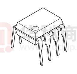
● Package Outline
■ PACKAGE OUTLINE
NJM4558D
NJM4559D
( DIP8 )
NJM4558M
NJM4559M
( DMP8 )
NJM4558V
( SSOP8 )
( ±4V~±18V )
( 100dB typ. )
( 5MΩ typ. )
NJM4558L
NJM4559L
( SIP8 )
NJM4558E
( SOP8 )
DIP8, DMP8, SIP8
SOP8 JEDEC 150mil (only NJM4558),
SSOP8 (only NJM4558)
■ PIN CONFIGURATION
( Top View )
1
8
A
2
A
B
7
B
3
4
6
5
NJM4558D, NJM4558M, NJM4558E, NJM4558V
NJM4559D, NJM4559M
1
2
3
4
5
NJM4558L
NJM4559L
6
7
8
PIN FUNCTION
1. A OUTPUT
2. A - INPUT
3. A +INPUT
4. V5. B +INPUT
6. B - INPUT
7. B OUTPUT
+
■ EQUIVALENT CIRCUIT ( 1/2 Shown )
V+
- INPUT
+ INPUT
OUTPUT
VVer.2011-12-12
-1-
�NJM4558/4559
■ ABSOLUTE MAXIMUM RATINGS
( Ta=25˚C )
PARAMETER
Supply Voltage
Differential Input Voltage
Input Voltage
SYMBOL
V+/VVID
VIC
Power Dissipation
PD
Operating Temperature Range
Storage Temperature Range
Topr
Tstg
RATINGS
± 18
± 30
± 15 ( note1 )
( DIP8 ) 500
( DMP8 ) 300
( SOP8 ) 300
( SSOP8 ) 250
( SIP8 ) 800
-40~+85
-40~+125
UNIT
V
V
V
mW
˚C
˚C
( note1 ) For supply voltage less than ±15V,the absolute maximum input voltage is equal to the supply voltage.
■ ELECTRICAL CHARACTERISTICS
( V+/V-=±15V,Ta=25˚C )
PARAMETER
Input Offset Voltage
Input Offset Current
Input Bias Current
Input Resistance
Large Signal Voltage Gain
Maximum Output Voltage Swing 1
Maximum Output Voltage Swing 2
Input Common Mode Voltage Range
Common Mode Rejection Ratio
Supply Voltage Rejection Ratio
Operating Current
Slew Rate
NJM4558
NJM4559
Equivalent Input Noise Voltage (note2)
Gain Bandwidth Product
NJM4558
NJM4559
SYMBOL
VIO
IIO
IB
RIN
AV
VOM1
VOM2
VICM
CMR
SVR
ICC
SR
SR
VNI
GB
TEST CONDITION
RS≤10kΩ
RL≥2kΩ,VO=±10V
RL≥10kΩ
RL≥2kΩ
RS≤10kΩ
RS≤10kΩ
RIAA,RS=2.2kΩ,30kHz LPF
MIN.
0.3
86
± 12
± 10
± 12
70
76.5
-
TYP.
0.5
5
25
5
100
± 14
± 13
14
90
90
3.5
MAX.
6
200
500
5.7
UNIT
mV
nA
nA
MΩ
dB
V
V
V
dB
dB
mA
-
1
2
1.4
-
V/μs
V/μs
μVrms
3
6
MHz
MHz
(note2) In regard to Noise Standard, NJRC is preparing for special D Rank type products (VNI=1.8µV max.) except for SSOP package.
-2-
Ver.2011-12-12
�NJM4558/4559
■ TYPICAL CHARACTERISTICS
Ver.2011-12-12
-3-
�NJM4558/4559
■ TYPICAL CHARACTERISTICS
[CAUTION]
The specifications on this databook are only
given for information , without any guarantee
as regards either mistakes or omissions. The
application circuits in this databook are
described only to show representative usages
of the product and not intended for the
guarantee or permission of any right including
the industrial rights.
-4-
Ver.2011-12-12
�
很抱歉,暂时无法提供与“NJM4558DD”相匹配的价格&库存,您可以联系我们找货
免费人工找货