www.msksemi.com
�LM358
Semiconductor
Compiance
GENERAL DESCRIPTION
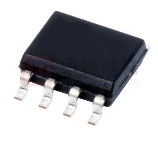
LM358 是一款双路低功耗的差分式运算放大器。具有单、双电源供电的特点。具有较高的开环增益、
内部补偿、高共模范围和良好的温度稳定性,以及具有输出短路保护的特点。可应用于传感器的放大电路、
直流放大模块,音频放大电路和传统的运算放大电路中。
FEATURES
●
内部频率补偿
●
高输入单电源电压范围:3V~36V
●
短路保护
●
高输入双电源电压范围:±18V
●
低功耗:单路典型值 300uA
●
单位增益带宽:大于 1.2MHZ
●
封装形式:DIP8、SOP8
●
●
音频放大器
其它应用领域
APPLICATION
●
●
传感器信号放大器
直流增益
PIN CONFIGURATION
DIP8/SOP8 管脚序号
管脚定义
功能说明
1
1OUT1
运放输出端
2
1IN-
运放输入负端
3
1IN+
运放输入正端
4
VEE
负电源端
5
2IN+
运放输入正端
6
2IN-
运放输入负端
7
2OUT
运放输出端
8
VCC
正电源端
www.msksemi.com
�LM358
Semiconductor
Compiance
极限参数
(2)
参数
符号
单电源供电电压
Vcc
40
V
双电源供电电压
Vs
±20
V
VIDR
±32
V
输入电压
VI
0.3~40V
V
输出短路时间
tsc
连续
耗散功率
PD
400
mW
工作温度
TA
0-70
℃
储存温度
TS
-65-150
℃
焊接温度
TW
260,10s
℃
(1)
差分输入电压
极限值
单位
注: (1)输入端NI+相对于IN-之间的最大电压差。
(2)极限参数是指无论在任何条件下都不能超过的极限值。如果超过此极限值,将有可能造成产品劣化等物理
性损伤;同时在接近极限参数下,不能保证芯片可以正常工作。
逻辑框图
www.msksemi.com
�LM358
Semiconductor
直流电学特性
Compiance
(TA=25℃,VCC=5V,VEE=GND 除非特别指定)
项目
符号
测试条件
最小值
典型值
最大值
单位
输入失调电压
VIO
VCC=5V to MAX,VIC=VICR(min),VO=1.4V
-
5
-
mV
输入失调电流
IIO
VO = 1.4 V
-
10
50
nA
偏置电流
IBIAS
VO = 1.4 V
-
50
250
nA
输入共模电压
VICR
VCC=5V to 36V
VEE
-
VCC-1.5V
V
输出高电压
VOH
VCC=28V,RL=2k
26
-
V
输出低电压
VOL
VCC=28V,RL=2k
-
0.85
-
V
开环电压增益
AOL
VCC=15V,VO=1V to 11V,RL≥2kΩ
70
100
-
V/mV
共模抑制比
CMRR
VCC=5V to MAX,VIC=VICR(min)
65
80
-
dB
单位增益带宽
GBWP
--
-
1.2
-
MHZ
电源电压抑制比 PSRR
∆VVDD/∆VIO
VCC=5V to MAX, f=20kHz
-
90
-
dB
串扰衰减抑制比 CS
VO1/VO2
f=1MHz
-
120
-
dB
VCC=15V,Iout =50uA
-
13.7
13.5
V
VCC=15V,Iout =1mA
-
13.6
13.3
V
VCC=15V,Iout =5mA
-
13.4
13
V
VCC=15V,Iout =50uA
-
0.1
0.15
V
VCC=15V,Iout =1mA
-
0.75
1
V
VCC=15V,Iout =5mA
-
1
1.5
V
VCC=5V,VEE=-5V,VO=0V
-
±24
-
mA
VCC=5V,VO=1/2VCC, No load
-
0.5
-
mA
VCC=36,VO=1/2VCC, No load
-
0.8
-
mA
-18
-
+18
V
VO+
电压输出幅值
VO-
输出短路电流
IOS
电源工作电流
ICC
双电源电压
VS
/f=1kHz to 20kHz
VCC,VEE
典型应用
1、线路图
运算放大器在反相放大器中的典型应用图
www.msksemi.com
�LM358
Semiconductor
Compiance
2、设计要求
必须选择大于输入电压范围和输出范围的电源电压。
例如,将信号源 VIN 从±0.5 V 放大到±1.8V。将电源设置为±5V 足以适应此应用要求。
3、设计过程
根据公式(1)计算放大倍数(增益) AV
AV =-VO/VIN
------(1)
AV =-VO/VIN=-1.8/0.5=-3.6
一旦确定了所需的增益 AV,就要为 RI 或 RF 电阻选择一个值。根据运放的电特性及功耗的需要,
可选择 1kΩ-100kΩ范围内的值。本例将选择 RI=10 kΩ,则 RF=36kΩ。这由方程式 2 确定。
AV =-RF/RI --------(2)
RF= -AV * RI=3.6*10 = 36 kΩ
4、应用曲线图
反相放大器的输入电压 VS 输出电压
www.msksemi.com
�LM358
Semiconductor
Compiance
PACKAGE MECHANICAL DATA
Symbol
A
A1
A2
b
c
D
e
E
E1
L
θ
Dimensions In Millimeters
Min
1.350
Max
1.750
Dimensions In Inches
Min
0.053
Max
0.069
0.100
0.250
1.350
1.550
0.330
0.510
0.170
0.250
4.800
5.000
1.270(BSC)
0.004
0.010
0.053
0.061
0.013
0.020
0.007
0.010
0.189
0.197
0.050(BSC)
5.800
3.800
0.400
6.200
4.000
1.270
0.228
0.150
0.016
0.244
0.157
0.050
0°
8°
0°
8°
REEL SPECIFICATION
P/N
PKG
QTY
LM358
SOP-8
2500
www.msksemi.com
�LM358
Semiconductor
Compiance
DIP 8
B、8-pin plastic SOP (225mil)
www.msksemi.com
�LM358
Semiconductor
Compiance
Attention
■ Any and all MSKSEMI Semiconductor products described or contained herein do not have specifications
that can handle applications that require extremely high levels of reliability, such as life-support systems,
aircraft's control systems, or other applications whose failure can be reasonably expected to result in serious
physical and/or material damage. Consult with your MSKSEMI Semiconductor representative nearest you
before using any MSKSEMI Semiconductor products described or contained herein in such applications.
■ MSKSEMI Semiconductor assumes no responsibility for equipment failures that result from using products
at values that exceed, even momentarily, rated values (such as maximum ratings, operating condition ranges, or
other parameters) listed in products specificationsof any andall MSKSEMI Semiconductor products described
orcontained herein.
■ Specifications of any and all MSKSEMI Semiconductor products described or contained herein stipulate the
performance, characteristics, and functions of the described products in the independent state, and are not
guarantees of the performance, characteristics, and functions of the described products as mounted in the
customer’s products or equipment. To verify symptoms and states that cannot be evaluated in an independent
device, the customer should always evaluate and test devices mounted in the customer’sproducts orequipment.
■ MSKSEMI Semiconductor. strives to supply high-quality high-reliability products. However, any and all
semiconductor products fail with someprobability. It is possiblethat these probabilistic failures could give rise to
accidents or events that could endanger human lives, that could give rise to smoke or fire, or that could cause
damage to other property. When designing equipment, adopt safety measures so that these kinds of accidents
or events cannot occur. Such measures include but are not limited to protective circuits anderror prevention
circuitsfor safedesign, redundant design, and structural design.
■ In the event that any or all MSKSEMI Semiconductor products(including technical data, services) described
or contained herein are controlled under any of applicable local export control laws and regulations, such
products must not be exported without obtaining the export license from theauthorities concerned in
accordance with the above law.
■ No part of this publication may be reproduced or transmitted in any form or by any means, electronic or
mechanical, including photocopying and recording, or any information storage or retrieval system, or otherwise,
without the prior written permission of MSKSEMI Semiconductor.
■ Information (including circuit diagrams and circuit parameters) herein is for example only ; it is not
guaranteed for volume production. MSKSEMI Semiconductor believes information herein is accurate and
reliable, but no guarantees are made or implied regarding its use or any infringementsof intellectual property
rights or other rightsof third parties.
■ Any and all information described or contained herein are subject to change without notice due to
product/technology improvement, etc. Whendesigning equipment, referto the "Delivery Specification" for the
MSKSEMI Semiconductor productthat you intend to use.
www.msksemi.com
�
