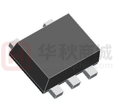
ESDA6V8AV5
ESDA6V8AV5
Http//:www.willsemi.com
4-Line, Low-Capacitor, Uni-directional
Transient Voltage Suppressors
Descriptions
The
ESDA6V8AV5
is
a
transient
voltage
suppressors (TVS) which provide a very high level
SOT-553
protection for sensitive electronic components that
may be subjected to electrostatic discharge (ESD). It is
designed to replace multiplayer varistors (MLV) in
I/O4
5
consumer equipments applications such as mobile
I/O3
4
phone, notebook, PAD, STB, LCD TV etc.
The ESDA6V8AV5 was past ESD transient
voltage
up
to
±8KV
(contact)
according
to
1
2
3
I/O1 GND I/O2
IEC61000-4-2 and withstand peak current up to 3A for
8/20us pulse according to IEC61000-4-5.
Pin configuration (Top view)
The ESDA6V8AV5 is available in SOT-553
package.
Standard
products
are
Pb-free
and
Halogen-free.
5
4
6H
Features
1
2
3
z
Working voltage
: 5V
6H = Device code
z
Peak power (tp=8/20us)
: 36W
*
z
ESD protection
Marking
IEC61000-4-2 (Contact)
: ±8KV
IEC61000-4-2 (Air)
: ±15KV
z
Low leakage current
z
Small package
Applications
z
Mobile phone
z
PAD
z
Notebook
z
STB
z
LCD TV
z
Digital camera
z
Other electronics equipments
Will Semiconductor Ltd.
= Month code (A~Z)
Order information
1
Device
Package
Shipping
ESDA6V8AV5-5/TR
SOT-553
3000/Tape&Reel
May, 2012 - Rev.2.1
�ESDA6V8AV5
Absolute maximum ratings
Parameter
Symbol
Rating
Unit
Peak pulse power (tp=8/20us)
Ppk
36
W
Peak pulse current (tp=8/20us)
Ipp
3
A
±8
KV
±15
KV
150
o
ESD voltage IEC61000-4-2 (Contact)
VESD
ESD voltage IEC61000-4-2 (Air)
Operation junction temperature
TJ
C
Lead temperature
TL
260
o
Storage temperature
Tsg
-55~150
o
C
C
Electronics characteristics (Ta=25 oC, unless otherwise noted)
Parameter
Symbol
Reveres maximum working voltage
VRWM
IR
Min.
Typ.
Max.
Unit
IR=1uA
5
V
VRWM=5V
1
uA
Reveres breakdown voltage
VBR
IT=1mA
6.2
6.8
7.5
V
Forward voltage
VF
IF=10mA
0.4
0.8
1.2
V
Clamping voltage
VC
Ipp=1A tp=8/20us
9
V
Ipp=3A tp=8/20us
12
V
Junction capacitance
CJ
16
20
pF
Junction capacitance
CJ
8
10
pF
110
100
90
80
70
60
50
40
30
20
10
0
I/O to GND,
VR=0V, F=1MHz
I/O to I/O
VR=0V, F=1MHz
100
90
Front times=1.25*( t90-t10) =8us
Peak Pulse Current (%)
Peak Pulse Current (%)
Reveres leakage current
Condition
Duration=20us
10
0
5
10
15
20
25
30
Peak Pulse time (us)
35
30ns
tr=0.7~1ns
40
8/20us waveform
Will Semiconductor Ltd.
60ns
IEC61000-4-2 waveform
2
May, 2012 - Rev.2.1
t
�ESDA6V8AV5
o
Typical characteristics (Ta=25 C, unless otherwise noted)
20
20
C - Junction capacitance (pF)
VC - Clamping voltage (V)
Pulse waveform: tp=8/20us
16
12
8
4
0
0
1
2
3
Fsignal =1MHz
18
Vsignal =50mVrms
16
14
12
10
8
6
4
0
Ipp - Peak pulse current (A)
Clamping voltage vs. Peak pulse current
1
2
3
4
5
VR - Reverse voltage (V)
Capacitance vs. Reveres voltage
1000
100
% of Rated power
Peak Pulse Power (W)
100
10
80
60
40
20
1
0
1
10
100
Pulse Duration(us)
1000
0
25
50
75
100
125
Non-Repetitive Peak Pulse Power vs. Pulse time
TA - Ambient temperature ( C)
Power derating vs. Temperature
ESD Clamping
ESD Clamping
(IEC61000-4-2 +8KV contact)
(IEC61000-4-2 -8KV contact)
Will Semiconductor Ltd.
150
o
3
May, 2012 - Rev.2.1
�ESDA6V8AV5
Package outline dimensions
SOT-553
Symbol
Dimensions in millimeter
Min.
Typ.
Max.
A
0.525
0.563
0.600
A1
0.000
0.025
0.050
e
0.450
0.500
0.550
c
0.090
0.125
0.160
D
1.500
1.600
1.700
b
0.170
0.220
0.270
E1
1.100
1.200
1.300
E
1.500
1.600
1.700
L
0.100
0.200
0.300
�
Will Semiconductor Ltd.
7eREF
4
May, 2012 - Rev.2.1
�
很抱歉,暂时无法提供与“ESDA6V8AV5”相匹配的价格&库存,您可以联系我们找货
免费人工找货