VS1602GMH
100V/130A N-Channel Advanced Power MOSFET
Features
Enhancement mode
V DS
100
V
R DS(on),TYP@ VGS=10 V
3.6
mΩ
I D(Wire bond limited)
130
A
Low RDS(on) to minimize conduction losses
VitoMOS® Ⅱ Technology
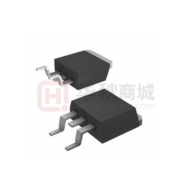
TO-263
100% Avalanche Tested, Rg 100% Tested
Part ID
Package Type
Marking
Packing
VS1602GMH
TO-263
1602GMH
800pcs/Reel
Maximum ratings, at TA =25°C, unless otherwise specified
Symbol
Parameter
Rating
Unit
V(BR)DSS
Drain-Source breakdown voltage
100
V
VGS
Gate-Source voltage
±20
V
IS
Diode continuous forward current (Wire bond limited)
TC = 25°C
130
A
ID
Continuous drain current @VGS=10V (Wire bond limited)
TC = 25°C
130
A
ID
Continuous drain current @VGS=10V (Silicon limited)
TC = 100°C
120
A
IDM
Pulse drain current tested ①
TC =25°C
675
A
TA=25°C
16
A
IDSM
Continuous drain current @VGS=10V
TA=70°C
12
A
484
mJ
EAS
Maximum Avalanche energy, single pulsed ②
PD
Maximum power dissipation ③
TC =25°C
250
W
PDSM
Maximum power dissipation ④
TA=25°C
2.1
W
TJ,TSTG
Operating junction and storage temperature range
-55 to 175
°C
Typical
Max
Unit
Thermal Characteristics
Symbol
Parameter
RθJC
Thermal Resistance, Junction-to-Case ⑤
0.5
0.6
°C/W
RθJA
Thermal Resistance, Junction-to-Ambient ⑥
50
60
°C/W
Copyright Vergiga Semiconductor Co., Ltd
Rev B – MAY, 2023
www.vgsemi.com
�VS1602GMH
100V/130A N-Channel Advanced Power MOSFET
Electrical Characteristics
Symbol
Parameter
Condition
Min.
Typ.
Max.
Unit
Static Electrical Characteristics @ Tj=25°C (unless otherwise stated)
V(BR)DSS
Drain-Source Breakdown Voltage
VGS=0V, ID=250μA
100
--
--
V
Zero Gate Voltage Drain Current(Tj=25℃)
VDS=100V,VGS=0V
--
--
1
μA
Zero Gate Voltage Drain Current(Tj=125℃)⑦
VDS=100V,VGS=0V
--
--
100
μA
IGSS
Gate-Body Leakage Current
VGS=±20V,VDS=0V
--
--
±100
nA
VGS(th)
Gate Threshold Voltage
VDS=VGS,ID=250μA
2.5
3
3.5
V
--
3.6
4.5
mΩ
RDS(on)
Drain-Source On-State Resistance ⑧
--
4.7
--
mΩ
--
5195
--
pF
--
875
--
pF
--
30
--
pF
--
1.8
--
Ω
--
91
--
nC
--
25
--
nC
--
25
--
nC
--
21
--
ns
IDSS
VGS=10V, ID=40A
(Tj=100℃)⑦
Dynamic Electrical Characteristics @ Tj = 25°C (unless otherwise stated)
Ciss
Input Capacitance ⑦
Coss
Output Capacitance ⑦
Crss
Reverse Transfer Capacitance ⑦
Rg
Gate Resistance
Qg
Total Gate Charge ⑦
Qgs
Gate-Source Charge ⑦
Qgd
Gate-Drain Charge ⑦
VDS=50V,VGS=0V,
f=100KHz
f=1MHz
VDS=50V,ID=40A,
VGS=10V
Switching Characteristics ⑦
Td(on)
Turn-on Delay Time
Tr
Turn-on Rise Time
ID=40A,
--
69
--
ns
Td(off)
Turn-Off Delay Time
RG=3Ω,
--
57
--
ns
--
70
--
ns
Tf
Turn-Off Fall Time
VDD=50V,
VGS=10V
Source- Drain Diode Characteristics@ Tj = 25°C (unless otherwise stated)
VSD
Forward on voltage
ISD=40A,VGS=0V
--
0.8
1.2
V
Trr
Reverse Recovery Time ⑦
Isd=40A, VGS=0V
--
59
--
ns
Qrr
Reverse Recovery Charge ⑦
di/dt=100A/μs
--
71
--
nC
NOTE:
① Single pulse; pulse width ≤ 100μs.
② This maximum value is based on starting TJ = 25°C, L = 0.5mH, RG = 25Ω, IAS = 44A, VGS =10V;100% FT tested at L = 0.5mH, IAS = 22A.
③ The power dissipation Pd is based on Tj(max), using junction-to-case thermal resistance RθJC.
④ The power dissipation Pdsm is based on Tj(max), using junction-to-ambient thermal resistance RθJA.
⑤ Thermal resistance from junction to soldering point (on the exposed drain pad). These tests are performed on a cool plate.
⑥ The value of RθJA is measured with the device in a still air environment with TA =25°C.
⑦ Guaranteed by design, not subject to production testing.
⑧ Pulse width ≤ 380μs; duty cycle≤ 2%.
Copyright Vergiga Semiconductor Co., Ltd
Rev B – MAY, 2023
www.vgsemi.com
�VS1602GMH
100V/130A N-Channel Advanced Power MOSFET
Typical Characteristics
3.9
10V,9V,8V,7V,6V
VGS= 5V
90
VGS(TH), Gate -Source Voltage (V)
ID, Drain-Source Current (A)
120
Notes:
1. 250μs pulse test
2. Tj=25°C
60
VGS= 4.5V
30
ID= 250uA
3.6
3.3
Max
3.0
2.7
Typ
2.4
Min
2.1
1.8
1.5
1.2
0.9
0
0
1
2
3
4
5
6
0
7
25
VDS, Drain -Source Voltage (V)
75
100
125
150
175
200
175
200
Tj - Junction Temperature (°C)
Fig1. Typical Output Characteristics
Fig2. VGS(TH) Gate -Source Voltage Vs. Tj
100
2.5
VDS=5V
Normalized On Resistance
80
ID, Drain-Source Current (A)
50
60
40
125°
C
25°
C
20
2.0
VGS= 10V
ID= 40A
1.5
1.0
0.5
0
0
1
2
3
4
5
6
7
8
9
0
10
25
50
75
100
125
150
Tj - Junction Temperature (°C)
VGS, Gate -Source Voltage (V)
Fig4. Typical Normalized On-Resistance Vs. Tj
Fig3. Typical Transfer Characteristics
8
20
IDS= 40A
6
On Resistance (mΩ)
On Resistance (mΩ)
16
12
125°C
8
4
VGS=10V
4
2
25°C
0
0
0
2
4
6
8
10
12
VGS, Gate -Source Voltage (V)
Fig5. Typical On Resistance Vs Gate -Source Voltage
Copyright Vergiga Semiconductor Co., Ltd
Rev B – MAY, 2023
5
10
15
20
25
30
35
40
ID, Drain-Source Current (A)
Fig6. Typical On Resistance Vs Drain Current and Gate
www.vgsemi.com
�VS1602GMH
100V/130A N-Channel Advanced Power MOSFET
Typical Characteristics
10
Tj=125°C
Tj=25°C
RDS(ON) limited
1000
ID - Drain Current (A)
ISD, Reverse Drain Current (A)
100
100
10µs
100µs
10
1ms
1
10ms
1
TC=25°C
0.1
0.1
0
0.2
0.4
0.6
0.8
1
1.2
1.4
0.1
1.6
1
10
100
VDS, Drain -Source Voltage (V)
VSD, Source-Drain Voltage (V)
Fig7. Typical Source-Drain Diode Forward Voltage
Fig8. Maximum Safe Operating Area
10
C, Capacitance (pF)
10000
VGS, Gate-Source Voltage (V)
VDS= 50V
Ciss
Coss
1000
Crss
100
ID= 40A
8
6
4
2
Frequency=100 KHz
0
10
0.1
1
10
0
100
40
60
80
100
Qg - Total Gate Charge (nC)
VDS, Drain-Source Voltage (V)
Fig9. Typical Capacitance Vs. Drain-Source Voltage
Fig10. Typical Gate Charge Vs. Gate-Source Voltage
200
300
wire bond limited
-------- silicon limited
250
ID, Maximum Drain Current (A)
Ptot, Power Dissipation (W)
20
200
150
100
50
25
120
80
40
ID=f(TC);VGS≥10V
Ptot=f(TC)
0
0
0
160
50
75
100
125
150
175
TC - Case Temperature (°C)
Fig11. Power Dissipation Vs. Case Temperature
Copyright Vergiga Semiconductor Co., Ltd
Rev B – MAY, 2023
200
0
25
50
75
100
125
150
175
200
TC - Case Temperature (°C)
Fig12. Maximum Drain Current Vs. Case Temperature
www.vgsemi.com
�VS1602GMH
100V/130A N-Channel Advanced Power MOSFET
Typical Characteristics
D=Ton/T
TJ,PK=TC+PDM.ZθJC.RθJC
RθJC=0.5°C/W
In descending order
D=0.5,0.3,0.1,0.05,0.02,0.01,single pulse
1
Thermal Resistance
ZθJC Normalized Transient
10
0.1
0.01
0.001
0.0001
0.000001
0.00001
0.0001
0.001
0.01
0.1
1
10
Pulse Width (s)
Fig13 . Normalized Maximum Transient Thermal Impedance
Fig14. Unclamped Inductive Test Circuit and waveforms
Copyright Vergiga Semiconductor Co., Ltd
Rev B – MAY, 2023
Fig15. Switching Time Test Circuit and waveforms
www.vgsemi.com
100
�VS1602GMH
100V/130A N-Channel Advanced Power MOSFET
Marking Information
Vs
1602GMH
XXXYWW
1st line:
2nd line:
3rd line:
Vergiga Code(Vs)
, Vergiga Logo
Part Number(1602GMH)
Date code (XXXYWW)
XXX: Wafer Lot Number Code , code changed with Lot Number
Y:
Year Code, refer to table below
WW: Week Code (01 to 53)
Code
C
D
E
F
G
H
J
K
L
M
N
P
Q
R
S
T
Year
2015
2016
2017
2018
2019
2020
2021
2022
2023
2024
2025
2026
2027
2028
2029
2030
Copyright Vergiga Semiconductor Co., Ltd
Rev B – MAY, 2023
www.vgsemi.com
�VS1602GMH
100V/130A N-Channel Advanced Power MOSFET
TO-263 Package Outline Data
Symbol
Dimensions (unit: mm)
Notes:
Min
Typ
Max
1. Refer to JEDEC TO-263 variation AB
A
4.37
4.57
4.77
2. Dimension "D" and "E" do NOT include mold flash.
A1
1.22
1.27
1.42
Mold flash shall not exceed 0.127mm per side.
A2
2.49
2.69
2.89
A3
0.00
0.13
0.25
b
0.70
0.81
0.96
b1
1.17
1.27
1.47
c
0.30
0.38
0.53
D1
8.50
8.70
8.90
D2
6.60
--
--
E
9.86
10.16
10.36
E1
7.06
--
--
e
2.54 BSC
H
14.70
15.10
15.50
H2
1.07
1.27
1.47
L
2.00
2.30
2.60
L1
1.40
1.55
1.70
Copyright Vergiga Semiconductor Co., Ltd
Rev B – MAY, 2023
www.vgsemi.com
�