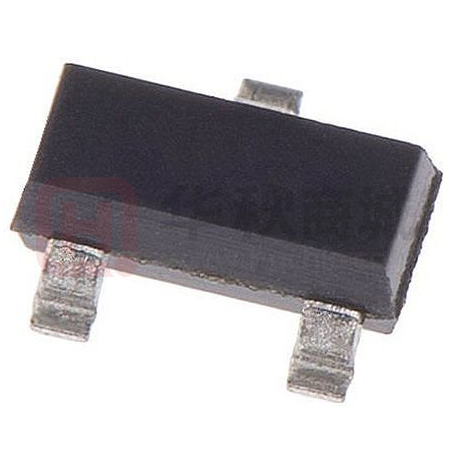
SI2301CDS-T1-GE3-ES
Rev-1.1
www.elecsuper.com
SuperMOS – SOT-23 -20V BVDSS, 58mΩ RDS(on),-3.0A ID P-channel MOSFET
1. Description
The SI2301CDS-T1-GE3-ES is P-Channel enhancement MOS Field Effect Transistor. Uses advanced
trench technology and design to provide excellent RDS(ON) with low gate charge. Device is suitable for
use in DC-DC conversion, power switch and charging circuit. Standard Product SI2301CDS-T1-GE3-ES
is Pb-free.
2. Features
-20V, RDS(ON)=58mΩ(Typ), VGS=-4.5V
Material: Halogen free
RDS(ON)=80mΩ(Typ), VGS=-2.5V
Reliable and rugged
Fast Switching
Avalanche Rated
High density cell design for low RDS(on)
Low leakage current
3. Applications
PWM applications
Power management in portable/desktop PCs
Load switch
DC/DC conversion
4. Ordering Information
Part Number
Package
Material
Quantity per reel
Flammability Rating
SI2301CDS-T1-GE3-ES
SOT-23
Halogen free
3,000 PCS
UL 94V-0
Table-1
Ordering information
5. Pin Configuration and Functions
Pin
Function
1
Gate
2
Source
3
Drain
Outline
3
1
Table-2
Copyright© ElecSuper Incorporated
Circuit Diagram
2
Pin configuration
Contact Us
1 / 6
�SI2301CDS-T1-GE3-ES
Rev-1.1
www.elecsuper.com
6. Specification
Absolute Maximum Rating & Thermal Characteristics
Ratings at 25 ℃ ambient temperature unless otherwise specified.
Parameter
Symbol
Limit
Unit
Drain-Source Voltage
BVDSS
-20
V
Gate-Source Voltage
VGS
±8
V
TA=25°C
Continuous Drain Current
TA=75°C
Maximum Power Dissipation
TA=25°C
TA=75°C
3.0
ID
A
1.7
1.4
PD
W
0.84
Pulsed Drain Current
IDM
9.2
A
Operating Junction Temperature
TJ
150
°C
Storage Temperature Range
Tstg
-55 to +150
°C
Thermal resistance ratings
Single Operation
Parameter
Junction-to-Ambient Thermal Resistance
Copyright© ElecSuper Incorporated
Contact Us
Symbol
Typical
Unit
RθJA
90
°C/W
2 / 6
�SI2301CDS-T1-GE3-ES
Rev-1.1
www.elecsuper.com
Electrical Characteristics
At TA = 25℃ unless otherwise specified
Parameter
Symbol
Test Conditions
Min.
Typ.
Max.
Unit
OFF CHARACTERISTICS
Drain-to-Source Breakdown Voltage
BVDSS
VGS=0V, ID=-250uA
-20
V
Zero Gate Voltage Drain Current
IDSS
VDS=-20V, VGS=0V
-1
uA
Gate-to-source Leakage Current
IGSS
VDS=0V, VGS=±8V
±100
nA
-0.7
-1.0
V
VGS=-4.5V, ID=-3.0A
58
75
VGS=-2.5V, ID=-2.0A
80
90
VDS=-5V, ID=-2.3A
6.5
ON CHARACTERISTICS
Gate Threshold Voltage
VGS(TH)
Drain-to-source On-resistance
RDS(on)
Forward trans conductance(a)
gfs
VGS=VDS, ID=-250uA
-0.4
mΩ
S
CHARGES, CAPACITANCES AND GATE RESISTANCE
Input Capacitance
CISS
Output Capacitance
COSS
Reverse Transfer Capacitance
CRSS
Gate Resistance
Total Gate Charge
Rg
f=1MHZ
QG(TOT)
Gate-to-Source Charge
QGS
Gate-to-Drain Charge
QGD
405
VGS=0V, VDS =-10V,
f=1MHz
VGS=-2.5V, VDS=-10V,
ID=-2.3A
75
pF
55
6
3.3
Ω
6
0.7
nC
1.3
SWITCHING CHARACTERISTICS
Turn-On Delay Time
Rise Time
Turn-Off Delay Time
Fall Time
td(ON)
tr
td(OFF)
VGS=-4.5V, VDS=10V,
RL=10Ω,ID=-1A,
RG=1Ω
tf
11
20
35
60
30
50
10
20
-0.8
-1.2
ns
BODY DIODE CHARACTERISTICS
Forward Voltage
Copyright© ElecSuper Incorporated
VSD
VGS=0V, IS=-1.0A
Contact Us
V
3 / 6
�SI2301CDS-T1-GE3-ES
7.
Rev-1.1
www.elecsuper.com
Typical Characteristic
Copyright© ElecSuper Incorporated
Contact Us
4 / 6
�SI2301CDS-T1-GE3-ES
Rev-1.1
www.elecsuper.com
8. Dimension (SOT-23)
θ
D
b
L1
3
E1
E
1
2
L
e
C
e1
A1
A
COMMON DIMENSIONS: UNITS OF MEASURE=MILLIMETER
Symbol
Dimensions
Symbol
Dimensions
Min.
Max.
A
0.900
1.150
E1
A1
0.900
1.050
e
b
0.300
0.500
e1
c
0.080
0.150
L
D
2.800
3.00
L1
0.300
0.500
E
1.200
1.400
θ
0°
8°
Copyright© ElecSuper Incorporated
Contact Us
Min.
Max.
2.250
2.550
0.950TYP
1.800
2.000
0.550REF
5 / 6
�SI2301CDS-T1-GE3-ES
Rev-1.1
www.elecsuper.com
DISCLAIMER
ELECSUPER PROVIDES TECHNICAL AND RELIABILITY DATA (INCLUDING DATASHEETS), DESIGN RESOURCES
(INCLUDING REFERENCE DESIGNS), APPLICATION OR OTHER DESIGN ADVICE, SAFETY INFORMATION, AND
OTHER RESOURCES “AS IS” AND WITH ALL FAULTS, AND DISCLAIMS ALL WARRANTIES, EXPRESS AND IMPLIED,
INCLUDING WITHOUT LIMITATION ANY IMPLIED WARRANTIES OF MERCHANTABILITY, FITNESS FOR A PARTICULAR
PURPOSE OR NON-INFRINGEMENT OF THIRD PARTY INTELLECTUAL PROPERTY RIGHTS.
These resources are intended for skilled developers designing with ElecSuper products. You are solely responsible for
(1) selecting the appropriate ElecSuper products for your application;
(2) designing, validating and testing your application;
(3) ensuring your application meets applicable standards, and any other safety, security, or other requirements.
These resources are subject to change without notice. ElecSuper grants you permission to use these resources only for
development of an application that uses the ElecSuper products described in the resource. Other reproduction and display of
these resources are prohibited. No license is granted to any other ElecSuper intellectual property right or to any third party
intellectual property right. ElecSuper disclaims responsibility for, and you will fully indemnify ElecSuper and its representatives
against, any claims, damages, costs, losses, and liabilities arising out of your use of these resources. ElecSuper’s products are
provided subject to ElecSuper’s Terms of Sale or other applicable terms available either on www.elecsuper.com or provided in
conjunction with such ElecSuper products. ElecSuper’s provision of these resources does not expand or otherwise alter
ElecSuper’s applicable warranties or warranty disclaimers for ElecSuper products.
Copyright© ElecSuper Incorporated
Contact Us
6 / 6
�
SI2301CDS-T1-GE3-ES 价格&库存
很抱歉,暂时无法提供与“SI2301CDS-T1-GE3-ES”相匹配的价格&库存,您可以联系我们找货
免费人工找货- 国内价格
- 1+0.30360
- 200+0.10120
- 1500+0.06325
- 3000+0.05027
- 国内价格
- 10+0.07938
- 100+0.07161
- 300+0.06729
- 3000+0.06459
- 6000+0.06243
- 9000+0.06113
