Flash Storage Specification e•MMC™ 5.1
Flash Storage Specification
e•MMC™ 4.5
Flash Storage Specification
e•MMC™ 4.5
Embedded Multimedia Card
(e•MMC™5.1 HS400)
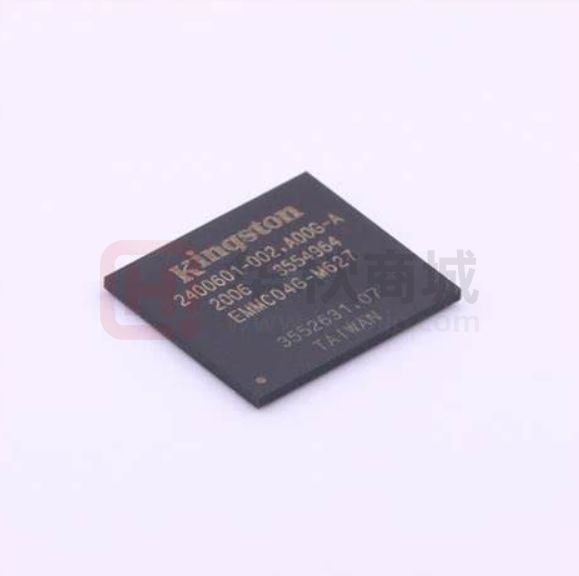
EMMC04G-M627
Datasheet
V1.0
Kingston Solutions Inc.
____________________________________________________________________________________________________________________
© 2016 Kingston Solutions Inc.
CONFIDENTIAL
1
�Flash Storage Specification e•MMC™ 5.1
Flash Storage Specification
e•MMC™ 4.5
Flash Storage Specification
e•MMC™ 4.5
CONTENTS
Product Features: ..................................................................................................................................................4
1. Introduction........................................................................................................................................................5
2. Specification .......................................................................................................................................................5
2.1. System Performance ....................................................................................................................................5
2.2. Power Consumption .....................................................................................................................................5
2.3. Capacity according to partition ................................................................................................................5
2.4. User Density ....................................................................................................................................................5
3. e•MMC™ Device and System ...........................................................................................................................6
3.1. e•MMC™ System Overview ..........................................................................................................................6
3.2. Memory Addressing .....................................................................................................................................6
3.3. e•MMC™ Device Overview ...........................................................................................................................7
3.3.1 Clock (CLK)..............................................................................................................................................7
3.3.2 Data Strobe(DS).....................................................................................................................................7
3.3.3 Command (CMD) ...................................................................................................................................7
3.3.4 Input/Outputs (DAT0-DAT7) ...........................................................................................................7
3.4. Bus Protocol ....................................................................................................................................................8
3.5. Bus Speed Modes ...........................................................................................................................................8
3.5.1 HS200 Bus Speed Mode ......................................................................................................................9
3.5.2 HS200 System Block Diagram ..........................................................................................................9
3.5.3 HS400 Bus Speed mode ......................................................................................................................9
3.5.4 HS400 System Block Diagram ....................................................................................................... 10
4. e•MMC™ Functional Description ............................................................................................................... 11
4.1 e•MMC™ Overview....................................................................................................................................... 11
4.2 Boot Operation Mode ................................................................................................................................ 11
4.3 Device Identification Mode ..................................................................................................................... 11
4.4 Interrupt Mode ............................................................................................................................................ 11
4.5 Data Transfer Mode ................................................................................................................................... 11
4.6 Inactive Mode .............................................................................................................................................. 12
4.7 H/W Reset Operation ................................................................................................................................ 12
4.8 Noise Filtering Timing for H/W Reset ................................................................................................. 13
4.9 Field Firmware Update(FFU) ................................................................................................................. 14
4.10 Power off Notification for sleep .......................................................................................................... 15
4.11 Cache Enhancement Barrier ................................................................................................................ 16
4.12 Cache Flushing Policy ............................................................................................................................. 18
4.13 Command Queueing ................................................................................................................................ 19
5. Register Settings ............................................................................................................................................ 20
5.1. OCR Register ................................................................................................................................................ 20
5.2. CID Register .................................................................................................................................................. 20
5.3. CSD Register ................................................................................................................................................. 20
5.4. Extended CSD Register ............................................................................................................................. 20
5.5. RCA Register ................................................................................................................................................. 20
5.6. DSR Register ................................................................................................................................................. 20
____________________________________________________________________________________________________________________
© 2016 Kingston Solutions Inc.
CONFIDENTIAL
2
�Flash Storage Specification e•MMC™ 5.1
Flash Storage Specification
e•MMC™ 4.5
Flash Storage Specification
e•MMC21
™ 4.5
6. The e•MMC™ bus .............................................................................................................................................
6.1 Power-up ....................................................................................................................................................... 22
6.1.1 e•MMC™ power-up ............................................................................................................................. 22
6.1.2 e•MMC™ Power Cycling..................................................................................................................... 23
6.2 Bus Operating Conditions ....................................................................................................................... 24
6.2.1 Power supply: e•MMC™ .................................................................................................................... 24
6.2.2 e•MMC™ Power Supply Voltage ..................................................................................................... 25
6.2.3 Bus Signal Line Load ......................................................................................................................... 26
6.2.4 HS400 reference load ....................................................................................................................... 27
6.3 Bus Signal Levels ........................................................................................................................................ 28
6.3.1 Open-drain Mode Bus Signal Level .............................................................................................. 28
6.3.2 Push-pull mode bus signal level— e•MMC™.............................................................................. 28
6.3.3 Bus Operating Conditions for HS200 & HS400 ........................................................................ 29
6.3.4 Device Output Driver Requirements for HS200 & HS400 ................................................... 29
6.4 Bus Timing .................................................................................................................................................... 29
6.4.1 Device Interface Timings ................................................................................................................ 30
6.5 Bus Timing for DAT Signals During Dual Data Rate Operation.................................................. 31
6.6 Bus Timing Specification in HS200 Mode .......................................................................................... 32
6.7 Bus Timing Specification in HS400 mode .......................................................................................... 36
6.7.1 HS400 Device Input Timing ........................................................................................................... 36
6.7.2 HS400 Device Output Timing ........................................................................................................ 37
7. Package connections .................................................................................................................................... 39
8. Ball Assignment (153 ball) ......................................................................................................................... 41
9. Temperature ................................................................................................................................................... 42
10. Marking ............................................................................................................................................................. 42
11. Revision History ............................................................................................................................................. 43
____________________________________________________________________________________________________________________
© 2016 Kingston Solutions Inc.
CONFIDENTIAL
3
�Flash Storage Specification e•MMC™ 5.1
Flash Storage Specification
e•MMC™ 4.5
Flash Storage Specification
e•MMC™ 4.5
Product Features:
•
•
•
•
•
•
•
•
•
•
•
•
•
•
•
•
•
•
•
•
•
•
•
-
Packaged NAND flash memory with e•MMC™ 5.1 interface
Compliant with e•MMC™ Specification Ver.4.4, 4.41,4.5,5.0 & 5.1
Bus mode
High-speed e•MMC™ protocol
Clock frequency : 0-200MHz.
Ten-wire bus (clock, 1 bit command, 8 bit data bus) and a hardware reset.
Supports three different data bus widths : 1 bit(default), 4 bits, 8 bits
Data transfer rate: up to 52Mbyte/s (using 8 parallel data lines at 52 MHz)
Single data rate : up to 200Mbyte/s @ 200MHz
Dual data rate : up to 400Mbyte/s @ 200MHz
Operating voltage range :
VCCQ = 1.8 V/3.3 V
VCC = 3.3 V
Error free memory access
Internal error correction code (ECC) to protect data communication
Internal enhanced data management algorithm
Solid protection of sudden power failure safe-update operations for data content
Security
Support secure bad block erase commands
Enhanced write Protection with permanent and partial protection options
Quality
RoHS compliant (for detailed RoHS declaration, please contact your KSI representative.)
Supports Field Firmware Update(FFU)
Enhanced Device Life time
Support Pre EOL information
Optimal Size
Supports Production State Awareness
Supports Power Off Notification for Sleep
Supports HS400
Supports CMD queuing
Supports Cache barrier
Supports Cache Flushing report
RPMB throughput improve
Supports BKOP control
Supports HCI for CMD queuing
Supports Enhanced strobe
Supports secure write protection
____________________________________________________________________________________________________________________
© 2016 Kingston Solutions Inc.
CONFIDENTIAL
4
�Flash Storage Specification e•MMC™ 5.1
Flash Storage Specification
e•MMC™ 4.5
Flash Storage Specification
e•MMC™ 4.5
1. Introduction
Kingston e•MMC™ products follow the JEDEC e•MMC™ 5.1 standard. It is an ideal universal storage solution
for many electronic devices, including smartphones, tablets, PDAs, eBook readers, digital cameras,
recorders, MP3, MP4 players, electronic learning products, digital TVs and set-top boxes. E•MMC™ encloses
the MLC NAND and e•MMC™ controller inside as one JEDEC standard package, providing a standard
interface to the host. The e•MMC™ controller directly manages NAND flash, including ECC, wear-leveling,
IOPS optimization and read sensing.
Table 1 – Device Summary
NAND
Package
Density
Product
Part Number
EMMC04G-M627
04GB
Operating
voltage
VCC=3.3V,
VCCQ=1.8V/3.3V
FBGA153
2. Specification
2.1. System Performance
Table 2- Read/Write Performance
Typical value
Products
Read Sequential (MB/s)
Write Sequential (MB/s)
EMMC04G-M627
250
25
Note 1: Values given for an 8-bit bus width, running HS400 mode from KSI proprietary tool, VCC=3.3V,VCCQ=1.8V.
Note 2: For performance number under other test conditions, please contact KSI representatives.
Note 3: Performance numbers might be subject to changes without notice.
2.2. Power Consumption
Products
Table 3–Device Power Consumption
Read(mA)
Write(mA)
VCCQ(1.8V)
VCC(3.3V)
VCCQ(1.8V)
VCC(3.3V)
Standby(mA)
EMMC04G-M627
85.7
37.3
34.9
22.6
0.13
Note 1: Values given for an 8-bit bus width, a clock frequency of 200MHz DDR mode, VCC= 3.3V±5%, VCCQ=1.8V±5%
Note 2: Standby current is measured at Vcc=3.3V±5% ,8-bit bus width without clock frequency.
Note 3: Current numbers might be subject to changes without notice.
2.3. Capacity according to partition
Capacity
Boot partition 1
Boot partition 2
RPMB
04 GB
2048 KB
2048 KB
512 KB
2.4. User Density
Total user density depends on device type.
For example , 52MB in the SLC mode requires 104 MB in MLC. This results in decreasing.
Device
User Density
4 GB
3825205248 Bytes
____________________________________________________________________________________________________________________
© 2016 Kingston Solutions Inc.
CONFIDENTIAL
5
�Flash Storage Specification e•MMC™ 5.1
Flash Storage Specification
e•MMC™ 4.5
Flash Storage Specification
e•MMC™ 4.5
3. e•MMC™ Device and System
3.1. e•MMC™ System Overview
The e•MMC™ specification covers the behavior of the interface and the Device controller. As part of this
specification the existence of a host controller and a memory storage array are implied but the
operation of these pieces is not fully specified.
Kingston NAND Device consists of a single chip MMC controller and NAND flash memory module. The
micro-controller interfaces with a host system allowing data to be written to and read from the NAND
flash memory module. The controller allows the host to be independent from details of erasing and
programming the flash memory.
Figure 1– e•MMC™ System Overview
3.2. Memory Addressing
Previous implementations of the e•MMC™ specification are following byte addressing with 32 bit field.
This addressing mechanism permitted for e•MMC™ densities up to and including 2 GB.
To support larger densities the addressing mechanism was update to support sector addresses (512 B
sectors). The sector addresses shall be used for all devices with capacity larger than 2 GB.
To determine the addressing mode use the host should read bit [30:29] in the OCR register.
____________________________________________________________________________________________________________________
© 2016 Kingston Solutions Inc.
CONFIDENTIAL
6
�Flash Storage Specification e•MMC™ 5.1
Flash Storage Specification
e•MMC™ 4.5
Flash Storage Specification
e•MMC™ 4.5
3.3. e•MMC™ Device Overview
The e•MMC™ device transfers data via a configurable number of data bus signals. The communication
signals are:
3.3.1 Clock (CLK)
Each cycle of this signal directs a one bit transfer on the command and either a one bit (1x) or a
two bits transfer (2x) on all the data lines. The frequency may vary between zero and the maximum
clock frequency.
3.3.2 Data Strobe(DS)
This signal is generated by the device and used for output in HS400 mode. The frequency of this
signal follows the frequency of CLK. For data output each cycle of this signal directs two bits
transfer(2x) on the data - one bit for positive edge and the other bit for negative edge. For CRC
status response output and CMD response output(enabled only HS400 enhanced strobe mode),
the CRC status is latched on the positive edge only, and don't care on the negative edge.
3.3.3 Command (CMD)
This signal is a bidirectional command channel used for Device initialization and transfer of
commands. The CMD signal has two operation modes: open-drain for initialization mode, and
push-pull for fast command transfer. Commands are sent from the e•MMC™ host controller to the
e•MMC™ Device and responses are sent from the Device to the host.
3.3.4 Input/Outputs (DAT0-DAT7)
These are bidirectional data channels. The DAT signals operate in push-pull mode. Only the Device
or the host is driving these signals at a time. By default, after power up or reset, only DAT0 is used
for data transfer. A wider data bus can be configured for data transfer, using either DAT0-DAT3 or
DAT0-DAT7, by the e•MMC™ host controller. The e•MMC™ Device includes internal pull-ups for
data lines DAT1-DAT7. Immediately after entering the 4-bit mode, the Device disconnects the
internal pull ups of lines DAT1, DAT2, and DAT3. Correspondingly, immediately after entering to
the 8-bit mode the Device disconnects the internal pull-ups of lines DAT1–DAT7.
Table 4– Communication Interface
Name
CLK
DAT0
DAT1
DAT2
DAT3
DAT4
DAT5
DAT6
DAT7
Type1
I
I/O/PP
Description
Clock
Data
Data
Data
Data
Data
Data
Data
Data
I/O/PP
I/O/PP
I/O/PP
I/O/PP
I/O/PP
I/O/PP
I/O/PP
____________________________________________________________________________________________________________________
© 2016 Kingston Solutions Inc.
CONFIDENTIAL
7
�Flash Storage Specification e•MMC™ 5.1
Flash Storage Specification
e•MMC™ 4.5
Flash Storage Specification
e•MMC™ 4.5
Command/Response
CMD
I/O/PP/OD
RST_n
I
Hardware reset
VCC
S
Supply voltage for Core
VCCQ
S
Supply voltage for I/O
VSS
S
Supply voltage ground for Core
VSSQ
S
Supply voltage ground for I/O
DS
O/PP
Data strobe
Note1:I: input; O: output; PP: push-pull; OD: open-drain; NC: Not connected (or logical high); S: power supply.
Table 5– e•MMC™ Registers
CID
Width
(Bytes)
16
RCA
2
DSR
2
CSD
16
OCR
4
Name
EXT_CSD
512
Description
Implementation
Device Identification number, an individual number for identification.
Relative Device Address is the Device system address, dynamically
assigned by the host during initialization.
Driver Stage Register, to configure the Device’s output drivers.
Device Specific Data, information about the Device operation
conditions.
Operation Conditions Register. Used by a special broadcast command
to identify the voltage type of the Device.
Extended Device Specific Data. Contains information about the Device
capabilities and selected modes. Introduced in standard v4.0
Mandatory
Mandatory
Optional
Mandatory
Mandatory
Mandatory
The host may reset the device by:
•
•
•
Switching the power supply off and back on. The device shall have its own power-on detection
circuitry which puts the device into a defined state after the power-on Device.
A reset signal
By sending a special command
3.4. Bus Protocol
After a power-on reset, the host must initialize the device by a special message-based e•MMC™ bus
protocol. For more details, refer to section 5.3.1 of the JEDEC Standard Specification No.JESD84-B51.
3.5. Bus Speed Modes
e•MMC™ defines several bus speed modes as shown in Table 6.
Table 6— Bus Speed Mode
Data Rate
IO Voltage
Bus Width
Frequency
Max Data Transfer
(implies x8 bus width)
Single
3.3/1.8V
1, 4, 8
0-26MHz
26MB/s
Single
3.3/1.8V
4, 8
0-52MHz
52MB/s
Dual
3.3/1.8V
4, 8
0-52MHz
104MB/s
HS200
Single
1.8V
4, 8
0-200MHz
200MB/s
HS400
Dual
1.8V
8
0-200MHz
400MB/s
Mode Name
Backwards
Compatibility with
legacy MMC card
High Speed SDR
High Speed DDR
____________________________________________________________________________________________________________________
© 2016 Kingston Solutions Inc.
CONFIDENTIAL
8
�Flash Storage Specification e•MMC™ 5.1
Flash Storage Specification
e•MMC™ 4.5
Flash Storage Specification
e•MMC™ 4.5
3.5.1 HS200 Bus Speed Mode
The HS200 mode offers the following features:
•
•
•
•
•
•
SDR Data sampling method
CLK frequency up to 200MHz Data rate – up to 200MB/s
8-bits bus width supported
Single ended signaling with 4 selectable Drive Strength
Signaling levels of 1.8V
Tuning concept for Read Operations
3.5.2 HS200 System Block Diagram
Figure 2 shows a typical HS200 Host and Device system. The host has a clock generator, which
supplies CLK to the Device. For write operations, clock and data direction are the same, write
data can be transferred synchronous with CLK, regardless of transmission line delay. For read
operations, clock and data direction are opposite; the read data received by Host is delayed by
round-trip delay, output delay and latency of Host and Device. For reads, the Host needs to have
an adjustable sampling point to reliably receive the incoming data
Figure 2— System Block Diagram
3.5.3 HS400 Bus Speed mode
The HS400 mode has the following features
•
DDR Data sampling method
•
CLK frequency up to 200MHz, Data rate is – up to 400MB/s
•
Only 8-bit bus width supported
•
Signaling levels of 1.8V
•
Support up to 5 selective Drive Strength
•
Data strobe signal is toggled only for Data out and CRC response
____________________________________________________________________________________________________________________
© 2016 Kingston Solutions Inc.
CONFIDENTIAL
9
�Flash Storage Specification e•MMC™ 5.1
Flash Storage Specification
e•MMC™ 4.5
Flash Storage Specification
e•MMC™ 4.5
3.5.4 HS400 System Block Diagram
Figure 3 shows a typical HS400 Host and Device system. The host has a clock generator, which
supplies CLK to the Device. For read operations, Data Strobe is generated by device output circuit.
Host receives the data which is aligned to the edge of Data Strobe.
Figure 3- HS400 Host and Device block diagram
____________________________________________________________________________________________________________________
© 2016 Kingston Solutions Inc.
CONFIDENTIAL
10
�Flash Storage Specification e•MMC™ 5.1
Flash Storage Specification
e•MMC™ 4.5
Flash Storage Specification
e•MMC™ 4.5
4. e•MMC™ Functional Description
4.1 e•MMC™ Overview
All communication between host and device are controlled by the host (main chip). The host sends a
command, which results in a device response. For more details, refer to section 6.1 of the JEDEC
Standard Specification No.JESD84-B51.
Five operation modes are defined for the e•MMC™ system:
•
•
•
•
•
Boot operation mode
Device identification mode
Interrupt mode
Data transfer mode
Inactive mode
4.2 Boot Operation Mode
In boot operation mode, the master (e•MMC™ host) can read boot data from the slave (e•MMC™ device)
by keeping CMD line low or sending CMD0 with argument + 0xFFFFFFFA, before issuing CMD1. The
data can be read from either boot area or user area depending on register setting. For more details,
refer to section 6.3 of the JEDEC Standard Specification No.JESD84-B51.
4.3 Device Identification Mode
While in device identification mode the host resets the device , validates operation voltage range and
access mode, identifies the device and assigns a Relative device Address (RCA) to the device on the bus.
All data communication in the Device Identification Mode uses the command line (CMD) only. For more
details, refer to section 6.4 of the JEDEC Standard Specification No.JESD84-B51.
4.4 Interrupt Mode
The interrupt mode on the e•MMC™ system enables the master (e•MMC™ host) to grant the
transmission allowance to the slaves (Device) simultaneously. This mode reduces the polling load for
the host and hence, the power consumption of the system, while maintaining adequate responsiveness
of the host to a Device request for service. Supporting e•MMC™ interrupt mode is an option, both for
the host and the Device. For more details, refer to section 6.5 of the JEDEC Standard Specification
No.JESD84-B51.
4.5 Data Transfer Mode
When the Device is in Stand-by State, communication over the CMD and DAT lines will be performed
in push-pull mode. For more details, refer to section 6.6 of the JEDEC Standard Specification
No.JESD84-B51.
____________________________________________________________________________________________________________________
© 2016 Kingston Solutions Inc.
CONFIDENTIAL
11
�Flash Storage Specification e•MMC™ 5.1
Flash Storage Specification
e•MMC™ 4.5
Flash Storage Specification
e•MMC™ 4.5
4.6 Inactive Mode
The device will enter inactive mode if either the device operating voltage range or access mode is not
valid. The device can also enter inactive mode with GO_INACTIVE_STATE command (CMD15). The
device will reset to Pre-idle state with power cycle. For more details, refer to section 6.1 of the JEDEC
Standard Specification No.JESD84-B51.
4.7
H/W Reset Operation
Figure 4– H/W Reset Waveform
Note1: Device will detect the rising edge of RST_n signal to trigger internal reset sequence
Table 7– H/W Reset Timing Parameters
Symbol
Comment
tRSTW
RST_n pulse width
tRSCA
RST_n to Command time
tRSTH
RST_n high period (interval time)
Min
Max
Unit
1
[us]
2001
[us]
1
[us]
Note1:74 cycles of clock signal required before issuing CMD1 or CMD0 with argument 0xFFFFFFFA
____________________________________________________________________________________________________________________
© 2016 Kingston Solutions Inc.
CONFIDENTIAL
12
�Flash Storage Specification e•MMC™ 5.1
4.8
Noise Filtering Timing for H/W Reset
Flash Storage Specification
e•MMC™ 4.5
Flash Storage Specification
e•MMC™ 4.5
Device must filter out 5ns or less pulse width for noise immunity
Figure 5– Noise Filtering Timing for H/W Reset
Device must not detect these rising edge.
Device must not detect 5ns or less of positive or negative RST_n pulse.
Device must detect more than or equal to 1us of positive or negative RST_n pulse width.
____________________________________________________________________________________________________________________
© 2016 Kingston Solutions Inc.
CONFIDENTIAL
13
�Flash Storage Specification e•MMC™ 5.1
4.9
Flash Storage Specification
e•MMC™ 4.5
Flash Storage Specification
e•MMC™ 4.5
Field Firmware Update(FFU)
Field Firmware Updates (FFU) enables features enhancement in the field. Using this mechanism
the host downloads a new version of the firmware to the e.MMC device and, following a successful
download, instructs the e.MMC device to install the new downloaded firmware into the device.
In order to start the FFU process the host first checks if the e.MMC device supports FFU
capabilities by reading SUPPPORTED_MODES and FW_CONFIG fields in the EXT_CSD. If the e.MMC
device supports the FFU feature the host may start the FFU process. The FFU process starts by
switching to FFU Mode in MODE_CONFIG field in the EXT_CSD. In FFU Mode host should use closedended or open ended commands for downloading the new firmware and reading vendor proprietary
data. In this mode, the host should set the argument of these commands to be as defined in FFU_ARG
field. In case these commands have a different argument the device behavior is not defined and the
FFU process may fail. The host should set Block Length to be DATA_SECTOR_SIZE. Downloaded
firmware bundle must be DATA_SECTOR_SIZE size aligned (internal padding of the bundle might be
required).Once in FFU Mode the host may send the new firmware bundle to the device using one or
more write commands.
The host could regain regular functionality of write and read commands by setting MODE_CONFIG
field in the EXT_CSD back to Normal state. Switching out of FFU Mode may abort the firmware
download operation. When host switched back to FFU Mode, the host should check the FFU Status to
get indication about the number of sectors which were downloaded successfully by reading the
NUMBER_OF_FW_SECTORS_CORRECTLY_PROGRAMMED in the extended CSD. In case the number of
sectors which were downloaded successfully is zero the host should re-start downloading the new
firmware bundle from its first sector. In case the number of sectors which were downloaded
successfully is positive the host should continue the download from the next sector, which would
resume the firmware download operation.
In case MODE_OPERATION_CODES field is not supported by the device the host sets to NORMAL
state and initiates a CMD0/HW_Reset/Power cycle to install the new firmware. In such case the
device doesn’t need to use NUMBER_OF_FW_SECTORS_CORRECTLY_PROGRAMMED.
In both cases occurrence of a CMD0/HW_Reset/Power occurred before the host successfully
downloaded the new firmware bundle to the device may cause the firmware download process to be
aborted.
____________________________________________________________________________________________________________________
© 2016 Kingston Solutions Inc.
CONFIDENTIAL
14
�Flash Storage Specification e•MMC™ 5.1
Flash Storage Specification
e•MMC™ 4.5
Flash Storage Specification
e•MMC™ 4.5
4.10 Power off Notification for sleep
The host should notify the device before it powers the device off. This allows the device to better
prepare itself for being powered off. Power the device off means to turn off all its power supplies. In
particular, the host should issue a power off notification (POWER_OFF_LONG, POWER_OFF_SHORT )
if it intends to turn off both VCC and VCCQ power I or it may use to a power off notification
(SLEEP_NOTIFICATION ) if it intends to turn-off VCC after moving the device to Sleep state.
To indicate to the device that power off notification is supported by the host, a supporting host
shall first set the POWER_OFF_NOTIFICATION byte in EXT_CSD [34] to POWERED_ON (0x01). To
execute a power off, before powering the device down the host will changes the value to either
POWER_OFF_SHORT (0x02) or POWER_OFF_LONG (0x03). Host should waits for the busy line to be
de-asserted. Once the setting has changed to either 0x02 or 0x03, host may safely power off the
device.
The host may issue SLEEP_AWAKE (CMD5) to enter or to exit from Sleep state if
POWER_OFF_NOTIFICATION byte is set to POWERED_ON. Before moving to Standby state and then
to Sleep state, the host sets POWER_OFF_NOTIFICATION to SLEEP_NOTIFICATION and waits for the
DAT0 line de-assertion. While in Sleep (slp) state VCC (Memory supply) may be turned off as defined
in 4.1.6. Removing power supplies other than VCC while the device is in the Sleep (slp) state may
result in undefined device behavior. Before removing all power supplies, the host should transition
the device out of Sleep (slp) state back to Transfer state using CMD5 and CMD7 and then execute a
power off notification setting POWER_OFF_NOTIFICATION byte to either POWER_OFF_SHORT or
POWER_OFF_LONG.
If host continues to send commands to the device after switching to the power off setting (POWER
_OFF_LONG, POWER_OFF_SHORT or SLEEP_NOTIFICATION) or performs HPI during its busy conditio
n, the device shall restore the POWER_OFF_NOTIFICATION byte to POWERED_ON.
If host tries to change POWER_OFF_NOTIFICATION to 0x00 after writing another value there, a SWIT
CH_ERROR is generated.
The difference between the two power-off modes is how urgent the host wants to turn power off.
The device should respond to POWER_OFF_SHORT quickly under the generic CMD6 timeout. If more t
ime is acceptable, POWER_OFF_LONG may be used and the device shall respond to it within the POW
ER_OFF_LONG_TIME timeout.
While POWER_OFF_NOTIFICATION is set to POWERED_ON, the device expects the host to host shall:
•Keep the device power supplies alive (both VCC and VCCQ) and in their active mode
•Not power off the device intentionally before changing POWER_OFF_NOTIFICATION to either
POWER_OFF_LONG or POWER_OFF_SHORT
____________________________________________________________________________________________________________________
© 2016 Kingston Solutions Inc.
CONFIDENTIAL
15
�Flash Storage Specification e•MMC™ 5.1
Flash Storage Specification
e•MMC™ 4.5
Flash Storage Specification
e•MMC™ 4.5
•Not power off VCC intentionally before changing POWER_OFF_NOTIFICATION to
SLEEP_NOTIFICATION and before moving the device to Sleep state
Before moving to Sleep state hosts may set the POWER_OFF_NOTIFICATION byte to
SLEEP_NOTIFICATION (0x04) if aware that the device is capable of autonomously initiating
background operations for possible performance improvements. Host should wait for the busy line to
be de-asserted. Busy line may be asserted up the period defined in SLEEP_NOTIFICATION_TIME byte
in EXT_CSD [216]. Once the setting has changed to 0x04 host may set the device into Sleep mode
(CMD7+CMD5). After getting out from Sleep the POWER_OFF_NOTIFICATION byte will restore its
value to POWERED_ON. HPI may interrupt the SLEEP_NOTIFICATION operation. In that case
POWER_OFF_NOTIFICATION byte will restore to POWERED_ON.
4.11 Cache Enhancement Barrier
Barrier function provides a way to perform a delayed in-order flushing of a cached data. The
main motivation for using barrier commands is to avoid the long delay that is introduced by flush
commands. There are cases where the host is not interested in flushing the data right away, however
it would like to keep an order between different cached data batches. The barrier command enables
the host achieving the in-order goal but without paying the flush delay, since the real flushing can be
delayed by the device to some later idle time. The formal definition of the barrier rule is as follows:
Denote a sequence of requests Ri, i=0,..,N. Assuming a barrier is set between requests Rx and
Rx+1 (0