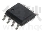
WPM9435
WPM9435
P-Channel Enhancement Mode MOSFET
www.willsemi.com
Description
The WPM9435 is the P-Channel logic enhancement mode
power field effect transistors are produced using high cell
density, DMOS trench technology.
This high density process is especially tailored to minimize
on-state resistance. These devices are particularly suited for low
voltage application, notebook computer power management and
other battery powered circuits where high-side switching.
Features
z
-30V/-5A,RDS(ON)= 36m@VGS=- 10V
z
-30V/-4A,RDS(ON)= 53m@VGS=-4.5V
z
Super high density cell design for extremely low RDS (ON)
z
Exceptional on-resistance and maximum DC current
capability
z
SOP – 8P package design
Application
z
Power Management in Note book
z
Portable Equipment
z
Battery Powered System
z
DC/DC Converter
z
Load Switch
D
D
D
D
S
S
S
G
WPM9435
YYWW
YYWW = Date Code
WPM9435 = Specific Device Code
Order information
3DUW�1XPEHU�
WPM9435-8/TR
http://www.willsemi.com
3DUW�1XPEHU�
SOP-8P
Page 1
6KLSSLQJ�
4000/ Tape&Reel
0 Jul, 2018 Rev 1.5
�WPM9435
PIN DESCRIPTION
Pin
Symbol
Description
1
2
3
4
5
6
7
8
S
S
S
G
D
D
D
D
Source
Source
Source
Gate
Drain
Drain
Drain
Drain
Absolute Maximum Ratings (TA=25 unless otherwise specified)
3DUDPHWHU�
6\PERO�
VDS
Drain-Source voltage
VGS
Gate-Source Voltage
ID
Continuous Drain Steady-State
TA=25ć
Current
Steady-State
TA=70ć
IDM
Pulse Drain Current
PD
Power Dissipation
TA=25ć
TA=70ć
TJ
Operating Junction Temperature Range
Tstg
Storage Temperature Range
RșJA
Thermal Resistance-Junction to Ambient
9DOXH�
-30
±20
-5.5
-4.4
-25
2.0
1.2
-55~150
8QLWV�
V
V
62.5
ć/W
A
A
W
ć
Electrical Characteristics
(TA=25к Unless otherwise noted)
Parameter
Symbol
Conditions
Min.
Typ
Max.
-2.0
-3.0
Unit
Static
Drain-Source Breakdown Voltage
Gate Threshold Voltage
V(BR)DSS VGS=0V,ID=-250uA
VGS(th) VDS=VGS,ID=-250uA
Gate Leakage Current
IGSS
Zero Gate Voltage Drain Current
IDSS
On-State Drain Current
ID(on)
Drain-Source On-Resistance
Forward Transconductance
Diode Forward Voltage
http://www.willsemi.com
RDS(on)
gfs
VSD
-30
-1.0
VDS=0V,VGS=±20V
VDS=-24V,VGS=0V
VDS=-24V,VGS=0V
TJ=85к
VDS= -5V,VGS =-4.5V
±100
-1
-10
-10
nA
uA
A
VGS=-10V,ID=-5.0A
VGS=-4.5V,ID=-4.0A
VDS=- 5V,ID=-5A
0.036
0.053
8
0.046
0.066
IS=-1.3A,VGS =0V
-0.79
-1.5
Page 2
V
ȍ
S
0 Jul, 2018 Rev 1.5
V
�WPM9435
Dynamic
Total Gate Charge
Qg
Gate-Source Charge
Qgs
Gate-Drain Charge
Qgd
Input Capacitance
Ciss
Output Capacitance
Coss
Reverse Transfer Capacitance
Crss
10
VDS=-15V,VGS=-10V
ID= -3.5A
tr
td(off)
Turn-Off Time
nC
1.6
3.0
710
VDS=-15V,VGS=0V
f=1MHz
pF
115
100
td(on)
Turn-On Time
18
VDD=-15V,RL=15ȍ
IDŁ-1.0A,VGEN=-10V
RG=6ȍ
tf
8
18
8
18
25
50
25
35
Typical Performance Characteristis
24
RDS(ON)ON Resistance(mOhm)
VGS=10V
150
ID,Drain Current(A)
20
VGS=6V
16
VGS=4V
12
8
VGS=3V
4
0
0
1
2
3
4
VDS,Drain-Source voltage(V)
5
VGS=4.5V
90
VGS=6V
60
V GS=10V
30
0
Drain Current VS Drain-Source voltage
http://www.willsemi.com
120
5
10
15
ID, Drain Current(A)
20
Drain Current vs ON Resistance
Page 3
0 Jul, 2018 Rev 1.5
nS
�WPM9435
25
VDS=2V
0.16
20
ID=-3A
ID,Drain Current(A)
RDS(ON) ON Resistance(Ohm)
0.20
0.12
0.08
15
10
5
0.04
0
0
2
4
6
8
VGS,Gate-Source Voltage(V)
10
1.5
2
3
4
5
6
VGS,Gate-Source Voltage(V)
1.6
Normalized On-Resistance
IS, Source-Drain Current(A)
1
Drain Current VS Gate-Source Voltage
Gate-Source Voltage vs ON Resistance
1.2
0.9
0.6
0.3
0.0
0.0
0
1.4
VGS=-10V
VGS=-4.5V
1.2
1
ID=-5A
0.8
0.2
0.4
0.6
VDS,Drain-Source voltage(V)
0.8
0
50
75
100
125
150
175
Temperature (°C)
On-Resistance vs. Junction
Drain Current VS Source-Drain Current
http://www.willsemi.com
25
Page 4
0 Jul, 2018 Rev 1.5
�WPM9435
1200
10
VDS=-15V
ID=-6A
9
8
1000
Capacitance (pF)
Ciss
-VGS (Volts)
7
6
5
4
3
2
800
600
400
Coss
200
1
Crss
0
0
0
2
4
6
8
10
12
14
16
0
5
10
-Qg (nC)
20
TJ(Max)=150°C
TA=25°C
TJ(Max)=150°C
TA=25°C
30
100Ps
Power (W)
-ID (Amps)
RDS(ON)
limited
1ms
0.1s
10ms
1
30
40
10Ps
10
25
Capacitance Characteristics
Gate-Charge Characteristics
100
15
-VDS (Volts)
1s
20
10
10s
DC
0
0.001
0.1
0.1
1
10
100
0.01
ZTJA Normalized Transient
Thermal Resistance
D=Ton/T
TJ,PK=TA+PDM.ZTJA.RTJA
RTJA=40°C/W
1
10
100
1000
Single Pulse Power Rating Junction-toAmbient (Note E)
Maximum Forward Biased Safe
Operating Area (Note E)
10
0.1
Pulse Width (s)
-VDS (Volts)
In descending order
D=0.5, 0.3, 0.1, 0.05, 0.02, 0.01, single pulse
1
THIS PRODUCT HAS BEEN DESIGNED AND QUALIFIED FOR THE CONSUMER MARKET. APPLICATIONS OR USES AS CRITICAL
PD
COMPONENTS
0.1 IN LIFE SUPPORT DEVICES OR SYSTEMS ARE NOT AUTHORIZED. AOS DOES NOT ASSUME ANY LIABILITY ARISING
OUT OF SUCH APPLICATIONS OR USES OF ITS PRODUCTS. AOS RESERVES THE RIGHT TO IMPROVE PRODUCT DESIGN,
Ton
FUNCTIONS AND RELIABILITY WITHOUT NOTICE.
T
Single Pulse
0.01
0.00001
0.0001
0.001
0.01
0.1
1
10
100
1000
Pulse Width (s)
Normalized Maximum Transient Thermal Impedance
http://www.willsemi.com
Page 5
0 Jul, 2018 Rev 1.5
�WPM9435
Packaging Information
SOP-8P Package Outline Dimension
http://www.willsemi.com
Page 6
0 Jul, 2018 Rev 1.5
�
很抱歉,暂时无法提供与“WPM9435-8/TR”相匹配的价格&库存,您可以联系我们找货
免费人工找货